

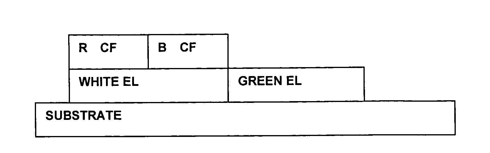
Organic EL panel
- Summary
- Abstract
- Description
- Claims
- Application Information
AI Technical Summary
Benefits of technology
Problems solved by technology
Method used
Image

Examples
Embodiment Construction
[0019] Preferred embodiments of the present invention will next be described referring to the drawings.
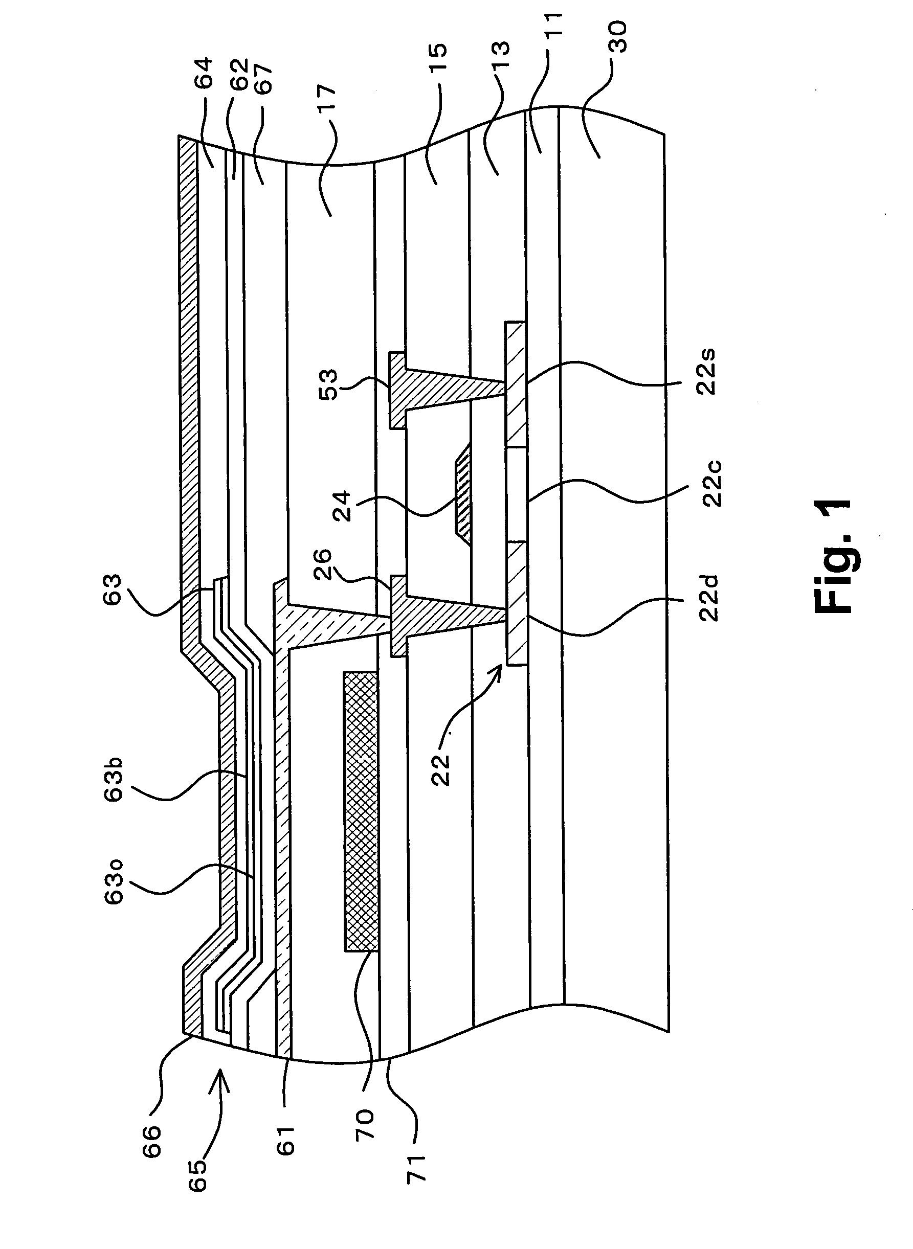
[0020]FIG. 1 is a cross-sectional view showing a configuration of a light-emitting region and a drive TFT (thin film transistor) within one pixel. It should be noted that each pixel actually includes a plurality of TFTs. The drive TFT is the TFT which controls a current supplied from a power line to an organic EL element within the pixel. On a glass substrate 30, a buffer layer 11 composed of a lamination of an SiN layer and an SiO2 layer is formed over the entire surface. Further on top, an active layer 22 made of polysilicon is disposed in predetermined areas (where TFTs are to be created).
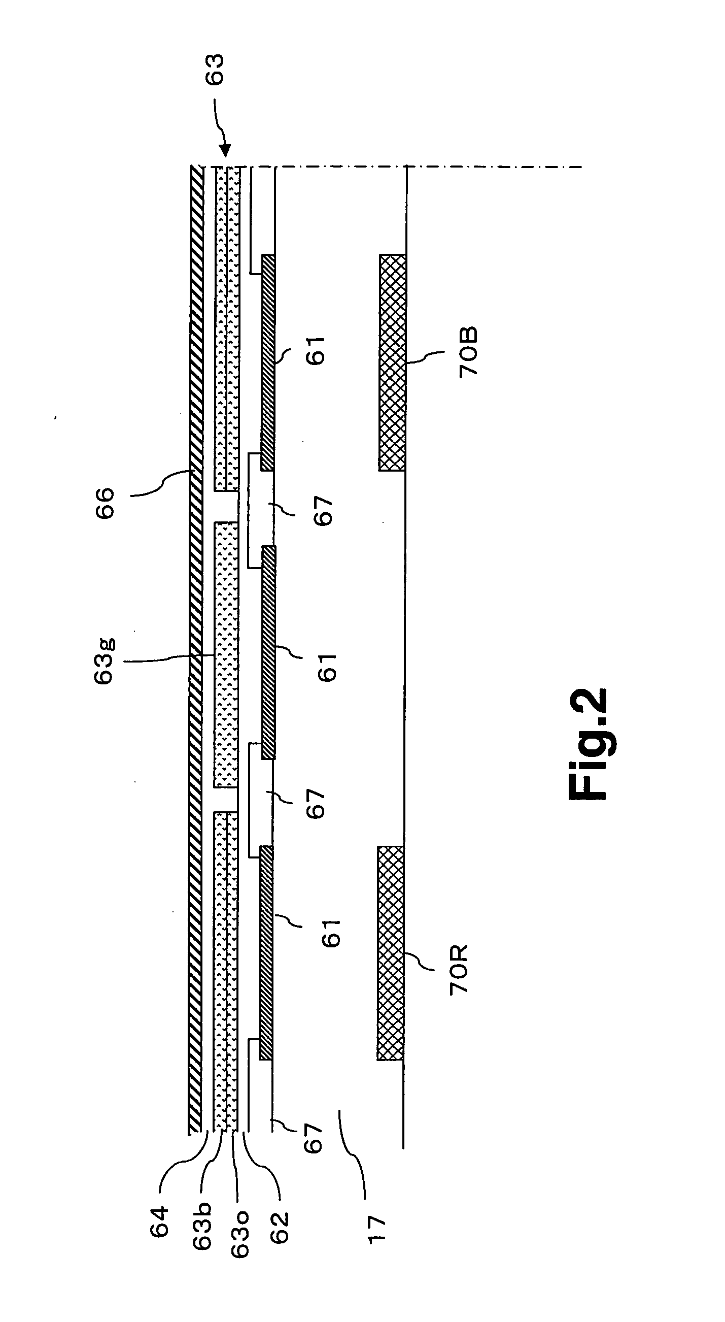
[0021] Covering the active layer 22 and the buffer layer 11, a gate insulation film 13 is formed over the entire surface. The gate insulation film 13 may be formed by laminating an SiO2 layer and an SiN layer. On top of the gate insulation film 13 at a position above a channel region 22c, a g...
PUM
| Property | Measurement | Unit |
|---|---|---|
| Color | aaaaa | aaaaa |
| Electric potential / voltage | aaaaa | aaaaa |
| Transport properties | aaaaa | aaaaa |
Abstract
Description
Claims
Application Information