Plasma display panel (PDP) with multiple dielectric layers
- Summary
- Abstract
- Description
- Claims
- Application Information
AI Technical Summary
Benefits of technology
Problems solved by technology
Method used
Image
Examples
Embodiment Construction
[0034] The present invention will now be described in more detail with reference to the appended drawings.
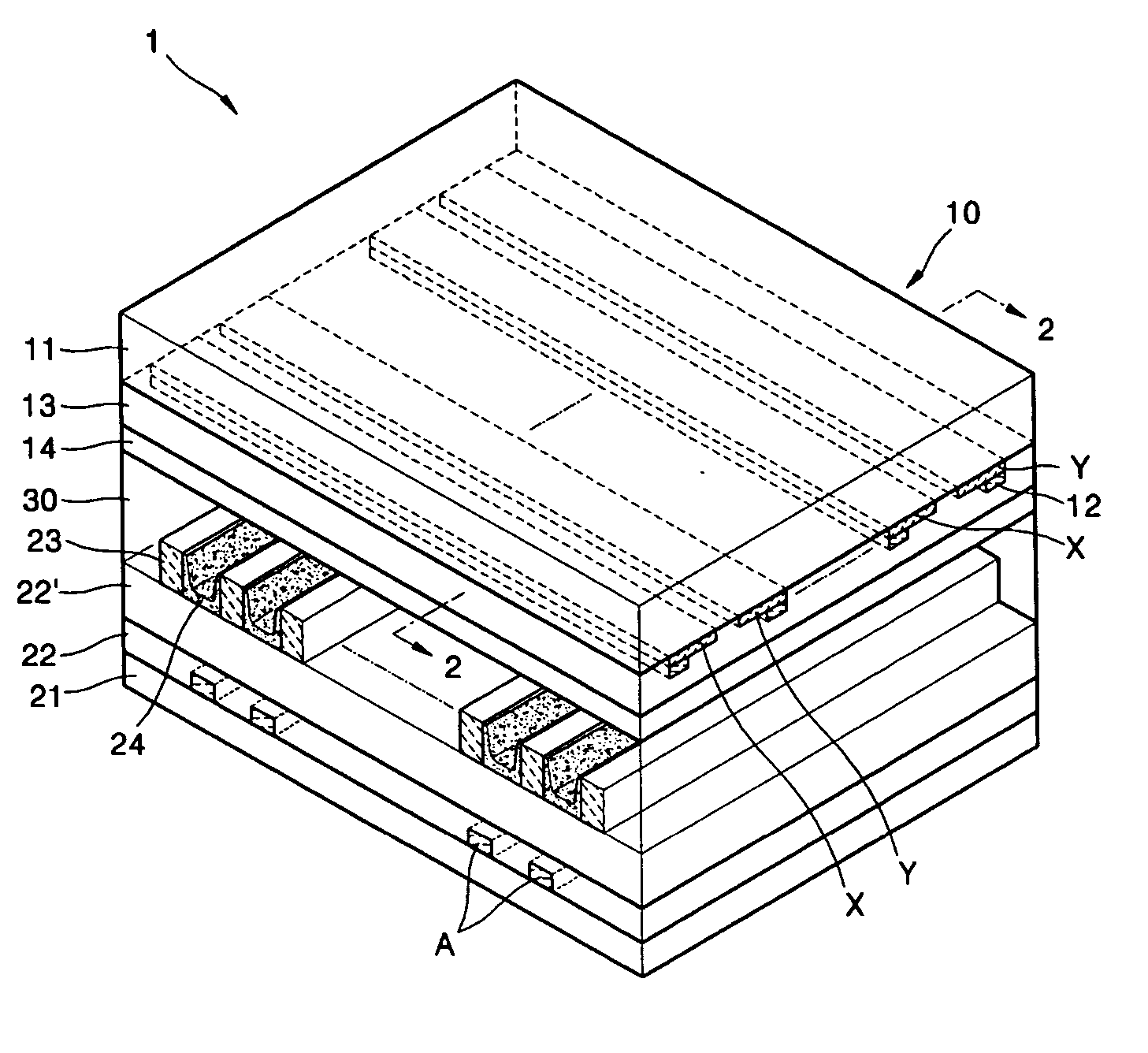
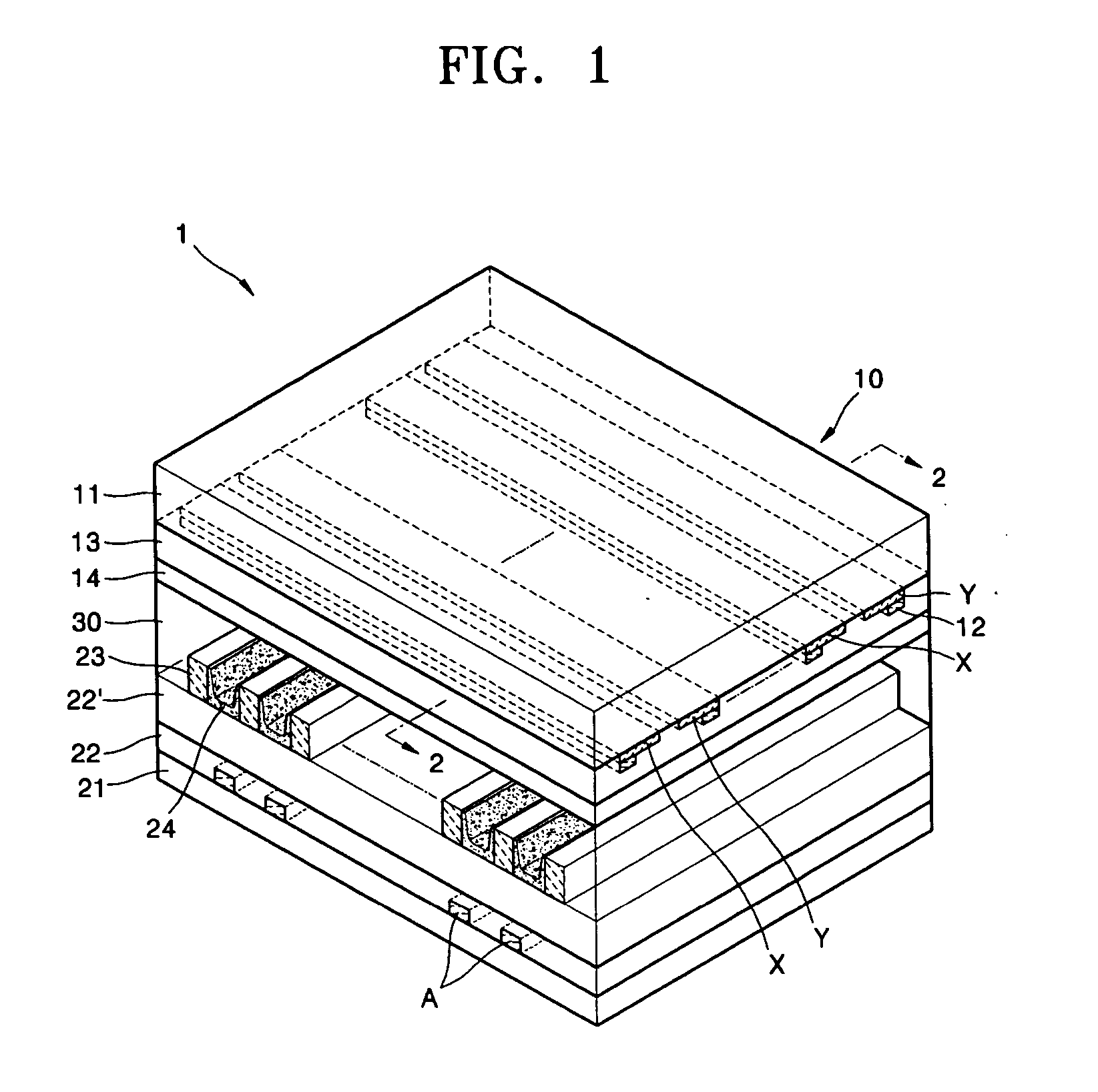
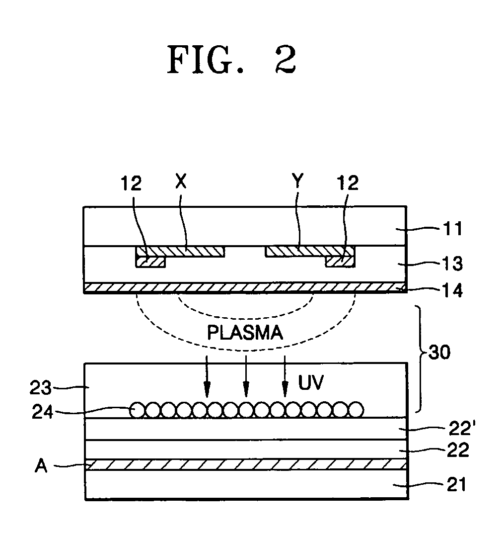
[0035]FIG. 1 is a perspective view of a PDP having dual back dielectric layers according to an embodiment of the present invention, and FIG. 2 is a cross-sectional view of the PDP taken along the line 2-2 of FIG. 1.
[0036] The PDP according to the present invention includes a front panel 10, a rear panel 20, and a plurality of discharge spaces 30. A plurality of sustain electrodes and scanning electrodes X and Y are arranged on one plane of a front substrate 11 of the front panel 10. Referring to FIG. 2, the sustain electrodes and the scanning electrodes have the same structures but have different voltage pulses supplied thereto. Bus electrodes 12 are arranged on and contact one plane of each of the plurality of sustain electrodes and scanning electrodes X and Y having a high transmissivity. The bus electrodes 12 have a low resistance and a uniform line width. A front dielectri...
PUM
 Abstract
Description
Claims
Application Information


