Gallium nitride compound semiconductor light emitting element and light source provided with said light emitting element

Active Publication Date: 2013-05-23
PANASONIC INTELLECTUAL PROPERTY MANAGEMENT CO LTD
View PDF3 Cites 3 Cited by
  • Summary
  • Abstract
  • Description
  • Claims
  • Application Information

AI Technical Summary

Benefits of technology

The patent text is about how to increase the brightness of a light.

Problems solved by technology

As a result, the probability of radiative recombination of carriers in the light-emitting layer decreases, thus decreasing the luminous efficiency as well.

Method used


Image

  • Gallium nitride compound semiconductor light emitting element and light source provided with said light emitting element
  • Gallium nitride compound semiconductor light emitting element and light source provided with said light emitting element
  • Gallium nitride compound semiconductor light emitting element and light source provided with said light emitting element

Examples


embodiment 1

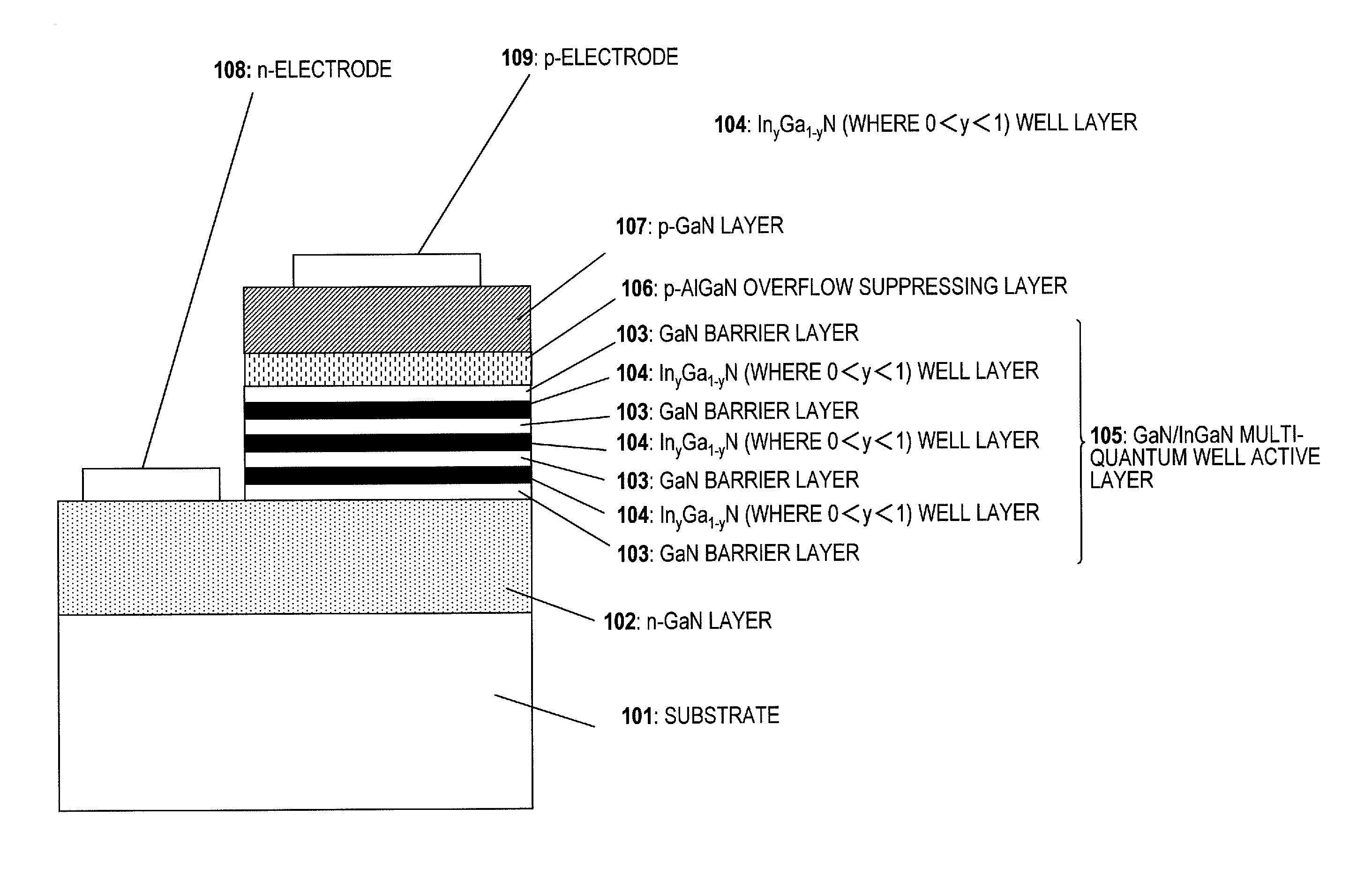
[0074]Hereinafter, a gallium nitride based compound semiconductor light-emitting element will be described as an embodiment of the present disclosure with reference to FIG. 7.

[0075]A crystal growing substrate 101 for use in this embodiment may be an m-plane GaN substrate, or an m-plane SiC substrate, of which the surface is covered with an m-plane GaN layer, or an r-plane or m-plane sapphire substrate, of which the surface is covered with an m-plane GaN layer. The point is that the active layer should be an m-plane nitride based semiconductor layer.

[0076]According to the present disclosure, the “m plane” may be a plane that tilts in a predetermined direction and defines a tilt angle of ±5 degrees or less with respect to an m plane that is not tilted. The growing plane of an actual m-plane semiconductor layer does not always have to be perfectly parallel to an m plane but may define a predetermined tilt angle with respect to the m plane. The tilt angle is defined by the angle that is...

embodiment 2

[0103]The light-emitting element of the embodiment described above may be used as a light source as it is. However, when combined with a resin including a phosphor to change the wavelength, for example, the light-emitting element of this embodiment can be used effectively as a light source having a broadened wavelength range (e.g., as a white light source).

[0104]FIG. 10 is a schematic representation illustrating an example of such a white light source. The light source shown in FIG. 10 includes the light-emitting element 100 having the configuration shown in FIG. 7 and a resin layer 200 in which a phosphor (such as YAG (yttrium aluminum garnet)) to change the wavelength of the light emitted from the light-emitting element 100 into a longer wavelength is dispersed. The light-emitting element 100 is mounted on a supporting member 220 on which an interconnect pattern has been formed. And on the supporting member 220, a reflective member 240 is arranged so as to surround the light-emitt...


PUM


Abstract

In a gallium nitride based compound semiconductor light-emitting element including an active layer, the active layer includes a well layer 104 and a barrier layer 103, each of which is a semiconductor layer of which the growing plane is an m plane. The well layer 104 has a lower surface and an upper surface and has an In composition distribution in which the composition of In changes according to a distance from the lower surface in a thickness direction of the well layer 104. The In composition of the well layer 104 becomes a local minimum at a level that is defined by a certain distance from the lower surface and that portion of the well layer 104 where the In composition becomes the local minimum runs parallel to the lower surface.

Description

[0001]This is a continuation of International Application No. PCT / JP2012 / 000214, with an international filing date of Jan. 16, 2012, which claims priority of Japanese Patent Application No. 2011-010906, filed on Jan. 21, 2011, the contents of which are hereby incorporated by reference.BACKGROUND[0002]1. Technical Field[0003]The present disclosure relates to a gallium nitride based compound semiconductor light-emitting element and also relates to a light source including the light-emitting element (which is typically a white light source).[0004]2. Description of the Related Art[0005]A nitride semiconductor including nitrogen (N) as a Group V element is a prime candidate for a material to make a short-wave light-emitting element, because its bandgap is sufficiently wide. Among other things, gallium nitride-based compound semiconductors (which will be referred to herein as “GaN-based semiconductors”) have been researched and developed particularly extensively. As a result, blue-ray-emi...

Claims


Application Information

Patent Timeline
IPC IPC(8): H01L33/32
CPCH01L33/007H01L33/16H01L33/32H01L33/06
Inventor KATO, RYOUYOSHIDA, SHUNJIYOKOGAWA, TOSHIYA
Owner PANASONIC INTELLECTUAL PROPERTY MANAGEMENT CO LTD
Why Eureka
Try Eureka