LED using thin film dichroic filters
- Summary
- Abstract
- Description
- Claims
- Application Information
AI Technical Summary
Benefits of technology
Problems solved by technology
Method used
Image
Examples
Embodiment Construction
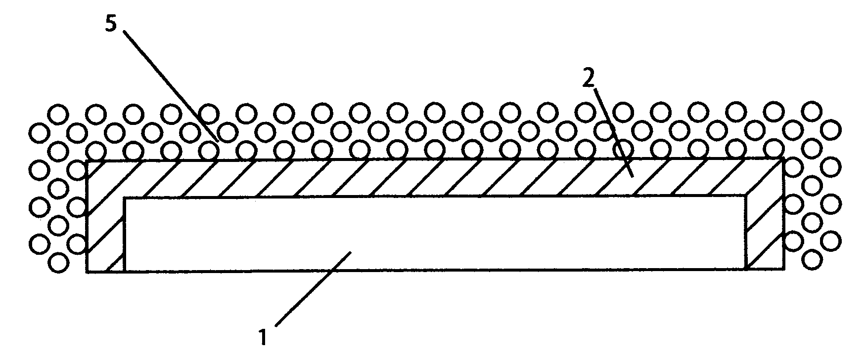
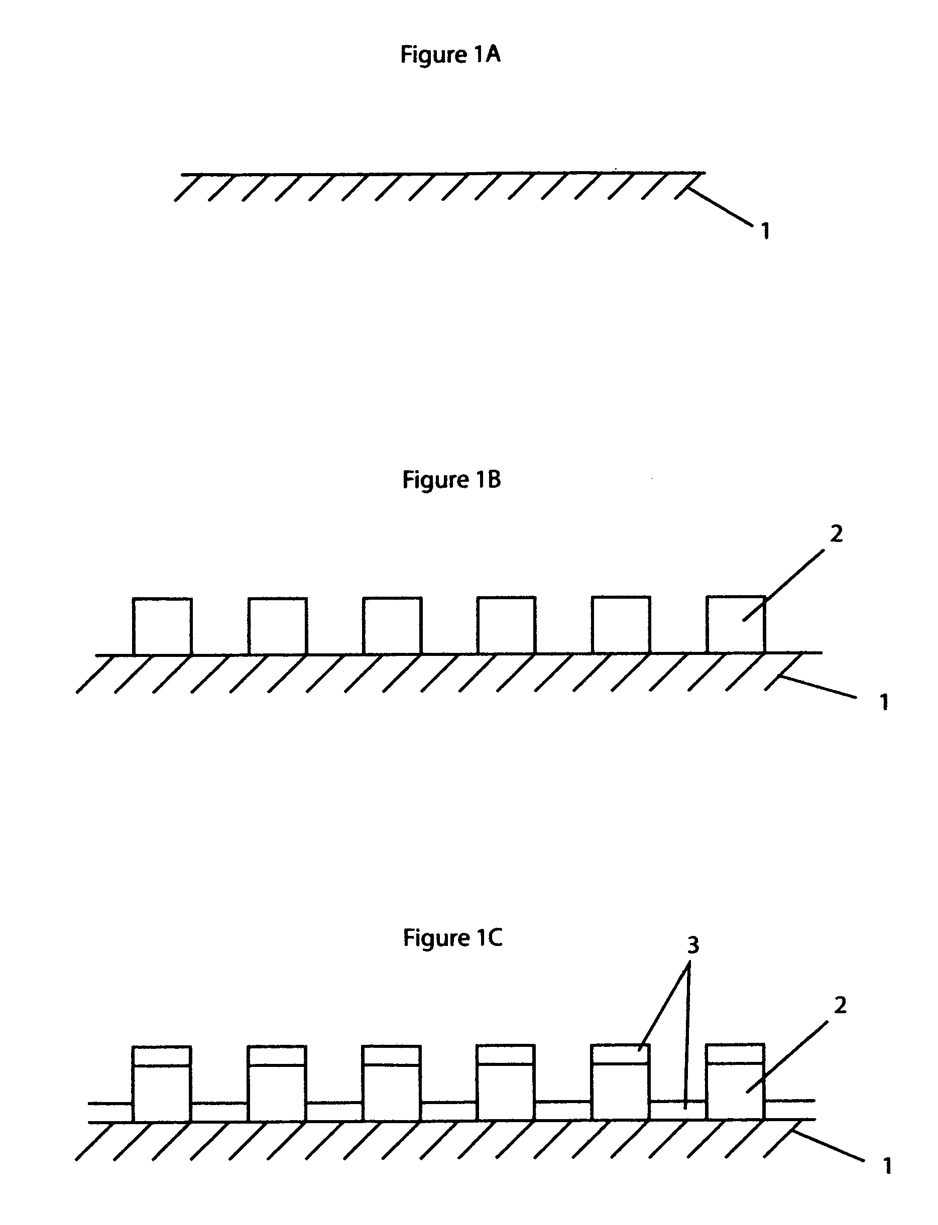
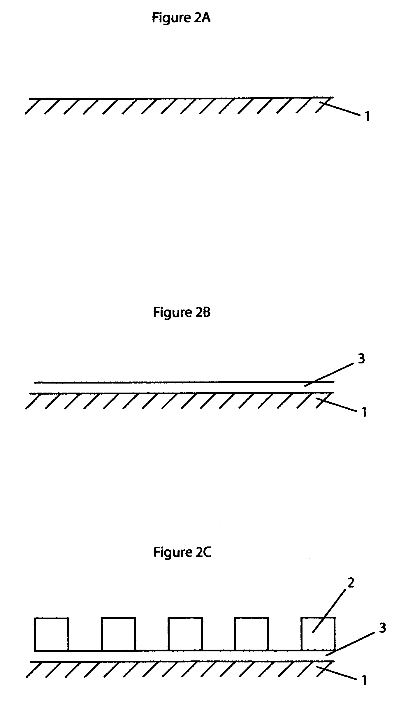
[0023]As shown in FIGS. 1a, 1b, and 1c the method and filter of this disclosure begins with the application and patterning of a photosensitive material (not shown) on a wafer substrate (1), more specifically, a LED wafer, as outlined in U.S. Pat. No. 5,711,889 but leaving off several dichroic layers of the patterned dichroic material (2) and replacing them with a blanket coating (3) such as an anti-reflective coating to complete the spectral characteristics desired. The steps as described in U.S. Pat. No. 5,711,899 are generally patterning photoresist on a wafer substrate (1) and masking pre-selected areas of said substrate via proximity, contact printing or other masking techniques well known in the art and coating a dichroic material (2) in the desired pattern. In most cases, but not all, multiple alternating layers of SiO2 and Ta2O5 are applied while lifting off the photoresist to form the patterned dichroic material (2). Then the whole surface is coated with an anti-reflective b...
PUM
 Abstract
Description
Claims
Application Information


