Plasma display panel and its driving method

Inactive Publication Date: 2005-04-28
PIONEER CORP
View PDF12 Cites 70 Cited by
  • Summary
  • Abstract
  • Description
  • Claims
  • Application Information

AI Technical Summary

Benefits of technology

[0055] A height of the stepped portion may preferably be in the range from 0.2 times to 0.9 times of a height of the discharge space at the center, and more preferably in the range from 0.6 times to 0.9 times of the height of the discharge space at the center. The adjustment to the height of the stepped portion makes it easy that an area of a low opposite discharge voltage is localized in the vicinity of the stepped portion. Upper surfaces of the stepped portion may be planarized, and a width of the planarized part with reference to a direction, along which the second electrode extends, may preferably be in the range of 0.2 times to 0.7 times of a length of the discharge cell in the direction, and more preferably in the range of 0.5 times to 0.7 times of the length of the discharge cell in the direction. This adjustment to the width of the planarized part of the stepped portion makes it easy to maintain a practically useful luminescent brightness and localizing an area of a low opposit

Problems solved by technology

This requires the increase in the current of the selective discharge, resulting in increases in the cost of the driving circuit and the power comsumption.
The selective discharge is caused over the entirety of the opposite discharge space, for which reason it is difficult to control the luminescent intensity and the minimum brightness of the selective discharge.
This means a deterioration of the luminescent performance.
In connection with the discharge gas including any of Xe, Kr, Ar and N

Method used


Image

  • Plasma display panel and its driving method
  • Plasma display panel and its driving method
  • Plasma display panel and its driving method

Examples


Example

FIRST EMBODIMENT

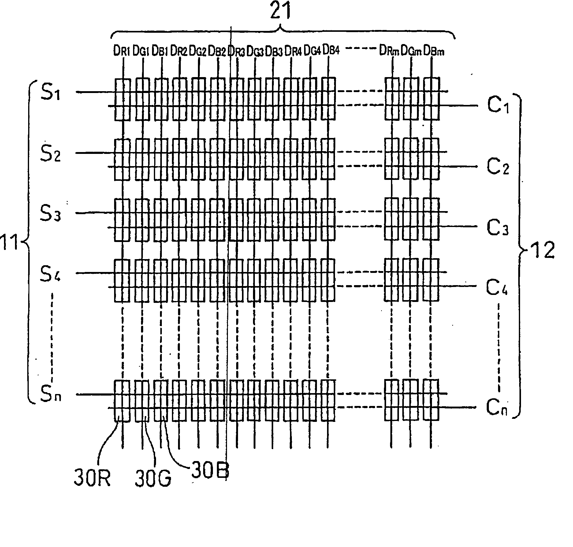
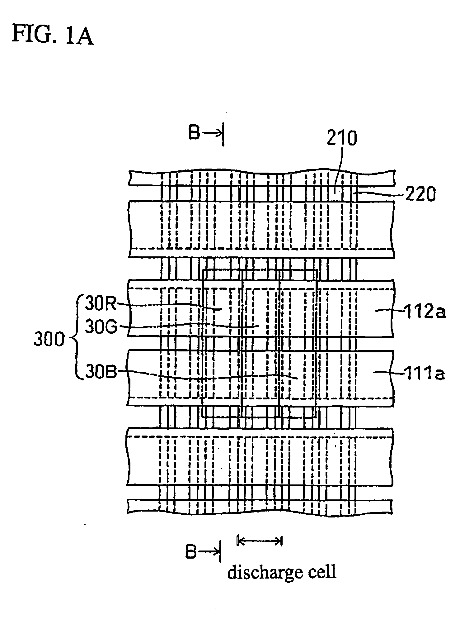
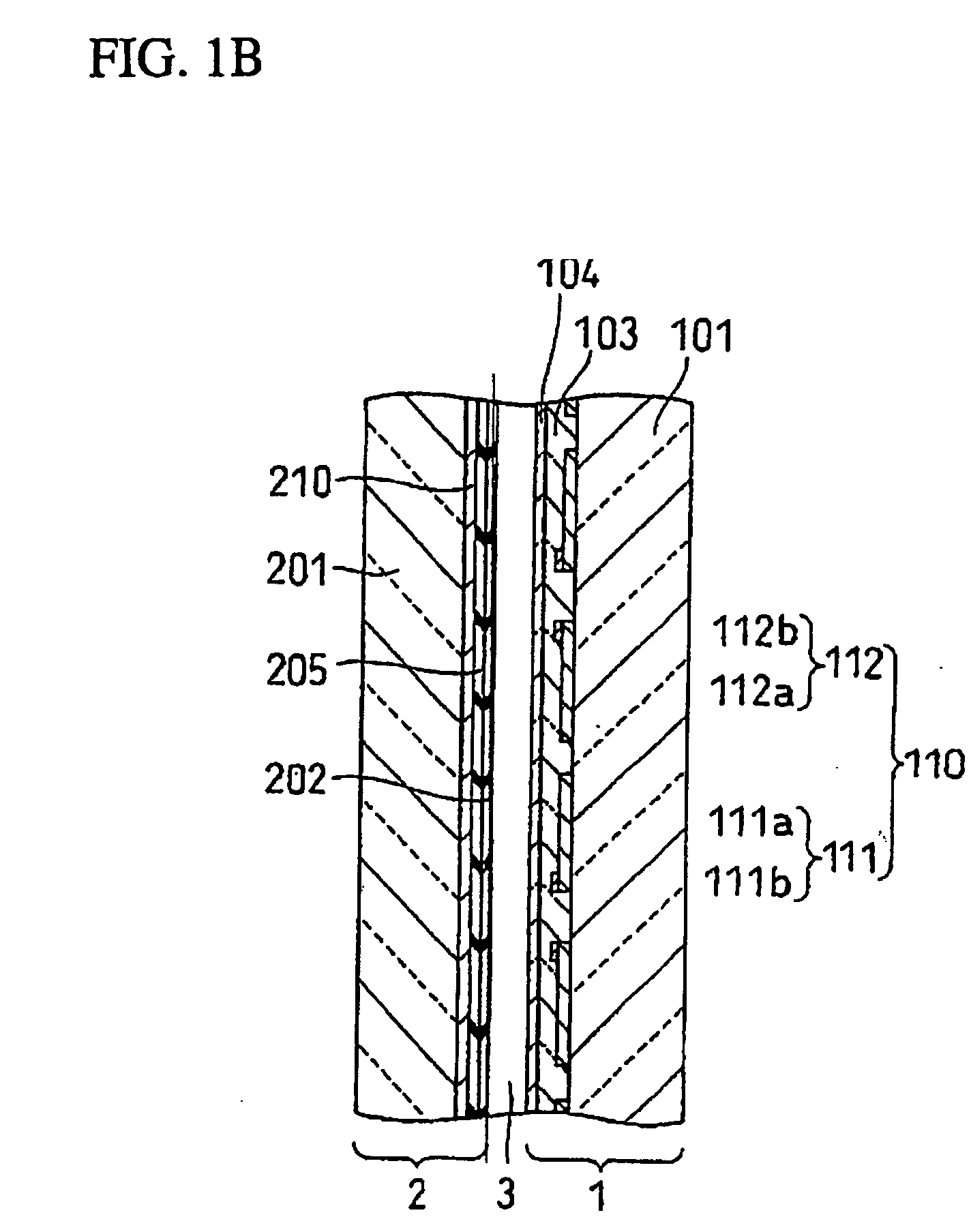
[0126]FIG. 8A is a fragmentary plan view showing a configuration of a plasma display panel in accordance with the first embodiment of the present invention. FIG. 8B is a fragmentary plan view showing a layout of electrodes in FIG. 8A. FIG. 9 is a fragmentary cross sectional view taken along an A-A line in FIGS. 8A and 8B.

[0127] In accordance with the first embodiment, the plasma display panel comprises a front substrate 1, a back substrate 2 and a discharge space defined between them. The front substrate 1 includes a first glass substrate 101, a plurality of surface discharge electrodes 110 and a plurality of light shielding layers 105. The surface discharge electrode 110 further includes a plurality of scanning electrodes 111 and a plurality of common electrodes 112, wherein the scanning electrodes 111 and the common electrodes 112 extend in a first horizontal direction and over the first glass substrate 101. The scanning electrode 111 further includes a transpare...

Example

[0158] A second embodiment of the present invention will be described. FIG. 13A is a fragmentary cross sectional view showing a discharge cell in a non-discharge state of the plasma display panel in accordance with the second embodiment of the present invention. FIG. 13B is a fragmentary cross sectional view showing a discharge cell in a weak initial discharge state of the plasma display panel in accordance with the second embodiment of the present invention. FIG. 13C is a fragmentary cross sectional view showing a discharge cell in a transitional discharge state of the plasma display panel in accordance with the second embodiment of the present invention. FIG. 13D is a fragmentary cross sectional view showing a discharge cell in a display discharge state of the plasma display panel in accordance with the second embodiment of the present invention. FIG. 14A is a fragmentary cross sectional view showing a discharge cell in a weak initial discharge state of the plasma display panel in...

Example

[0173] A third embodiment of the present invention will be described. In this third embodiment, the novel method of driving the conventional plasma display panel shown in FIGS. 7A, 7B, and 7C. FIG. 16 is a timing chart showing another method of driving the plasma display panel in accordance with the third embodiment of the present invention. FIG. 17A is a cross sectional view showing a uniform distribution of wall charges of a discharge cell of the plasma display panel in accordance with the third embodiment of the present invention. FIG. 17A is a cross sectional view showing a local distribution of wall charges of a discharge cell of the plasma display panel in accordance with the third embodiment of the present invention. FIG. 18A is a fragmentary cross sectional view showing a discharge cell in a non-discharge state of the plasma display panel in accordance with the third embodiment of the present invention. FIG. 18B is a fragmentary cross sectional view showing a discharge cell ...


PUM


Abstract

A plasma display panel and its driving method are provided, which is capable of improving high speed performance and reducing the necessary voltage for a selective discharge for switching a discharge cell and preferably of suppressing a brightness in a black display and making it easy to modulate the minimum brightness for improving the quality of image.
A scanning pulse voltage and a high-level data pulse voltage are so set that even if a data pulse of a discharge cell is low level or this discharge cell is non-selected, then in this non-selected discharge cell, a weak discharge 501 is generated between a low resistive wiring 111b and a stepped portion 203 over a data electrode 210 which are overlapped each other, and if a data pulse of a discharge cell is high level or this discharge cell is selected, then the weak discharge 501 is generated immediately after application of the data pulse before this discharge expends to a position under a transparent electrode 111a, whereby the weak discharge 501 becomes a discharge 502.

Description

TECHNICAL FIELD [0001] The present invention relates to a plasma display panel, and more particularly to a plasma display panel having an improvement in a quality of image, wherein the plasma display panel is used as a large-size plat panel display for a high definition television and a wall-mounted television, as well as for displays of a personal computer and a workstation. BACKGROUND OF THE ART [0002] An AC-luminescence plasma display panel of three-electrode surface-discharge type has the following configuration. The term “up-and-bottom directions” means directions, along which electrodes are formed with reference to a glass substrate. FIG. 1A is a fragmentary plan view showing arrangements of electrodes of a conventional plasma display panel. FIG. 1B is a fragmentary cross sectional elevation view, taken along a B-B line of FIG. 1A, showing a cross sectional structure of the conventional plasma display panel. [0003] The conventional plasma display panel comprises a front substr...

Claims


Application Information

Patent Timeline
IPC IPC(8): G09G3/20G09G3/28G09G3/288G09G3/291G09G3/292G09G3/293G09G3/294G09G3/298H01J11/12H01J11/14H01J11/24H01J11/26H01J11/32H01J11/36H01J11/44H01J11/50H04N5/66
CPCG09G3/2037G09G3/2927G09G3/294G09G2310/066H01J11/36G09G2320/0271H01J11/12H01J11/24G09G2320/0238H01J11/28
Inventor YOSHIOKA, TOSHIHIRO
Owner PIONEER CORP
Why Eureka
Try Eureka