Image processing device, image processing method and solid-state image-pickup device

Active Publication Date: 2005-04-28
ADVANCED INTERCONNECT SYST LTD
View PDF8 Cites 12 Cited by
  • Summary
  • Abstract
  • Description
  • Claims
  • Application Information

AI Technical Summary

Benefits of technology

[0012] According to this structure, the appropr

Problems solved by technology

However, the above Japanese Patent Publication Laid-Open No. 11-195778 does not disclose the control of a line for reading out an image signal or line for clearing an im

Method used


Image

  • Image processing device, image processing method and solid-state image-pickup device
  • Image processing device, image processing method and solid-state image-pickup device
  • Image processing device, image processing method and solid-state image-pickup device

Examples


Embodiment Construction

[0038] The preferred embodiments of the present invention are explained in detail referring to the drawings.

[0039] At first, an overall structure of an image processing device related to the present embodiments is explained referring to FIG. 1.

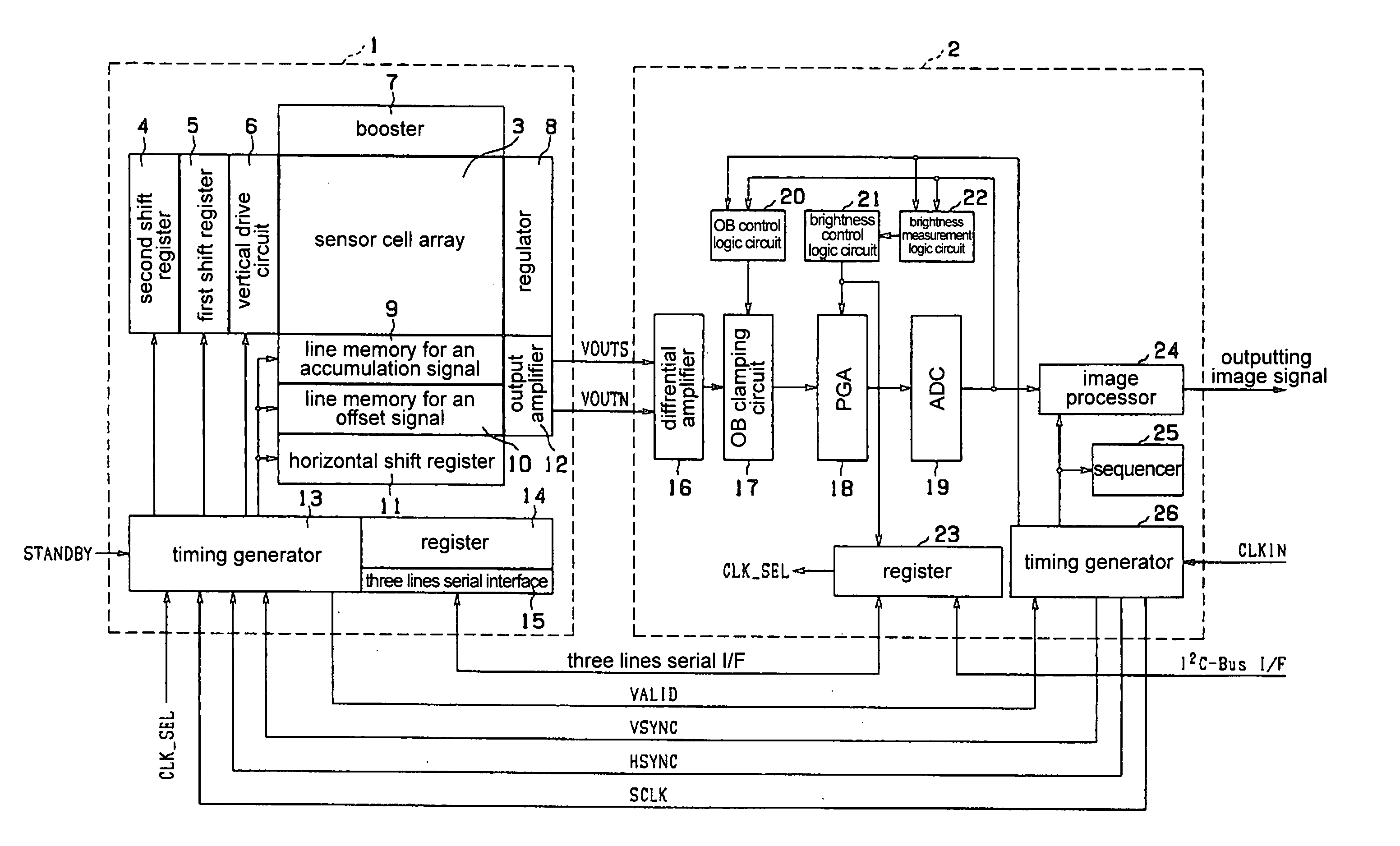
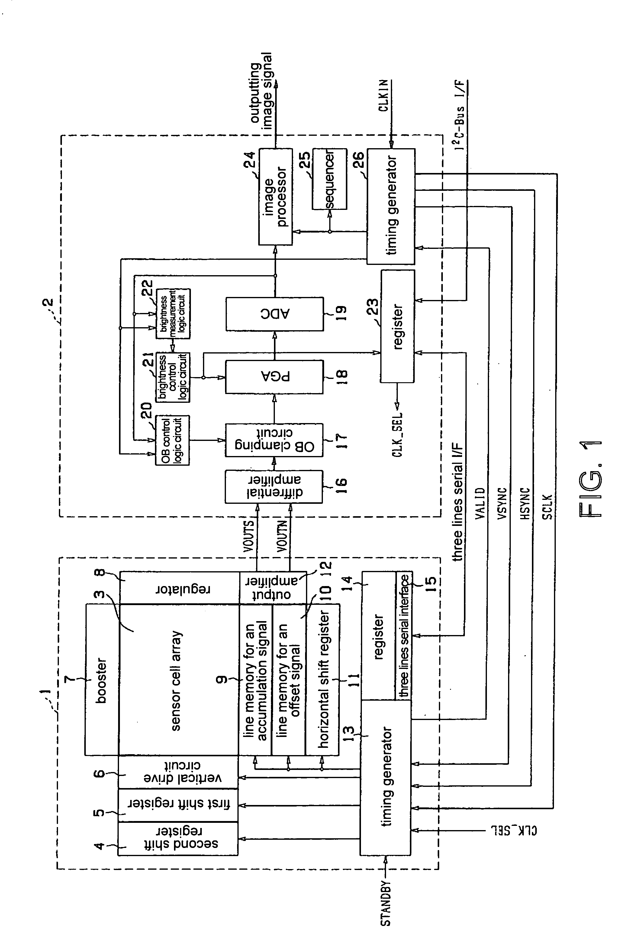
[0040]FIG. 1 shows a block diagram of the image processing device including an image sensor LSI (large scale integrated circuit) 1 as a solid-state image-pickup device and a signal processor LSI 2 as a signal processing device. The image sensor LSI 1 is a two-dimensional solid-state image-pickup device that converts an optical image to an electrical signal and applies this pixel signal based on the optical image to the signal processor LSI 2. The signal processor LSI 2 executes a predetermined signal processing to each of received pixel signals and outputs an image signal.

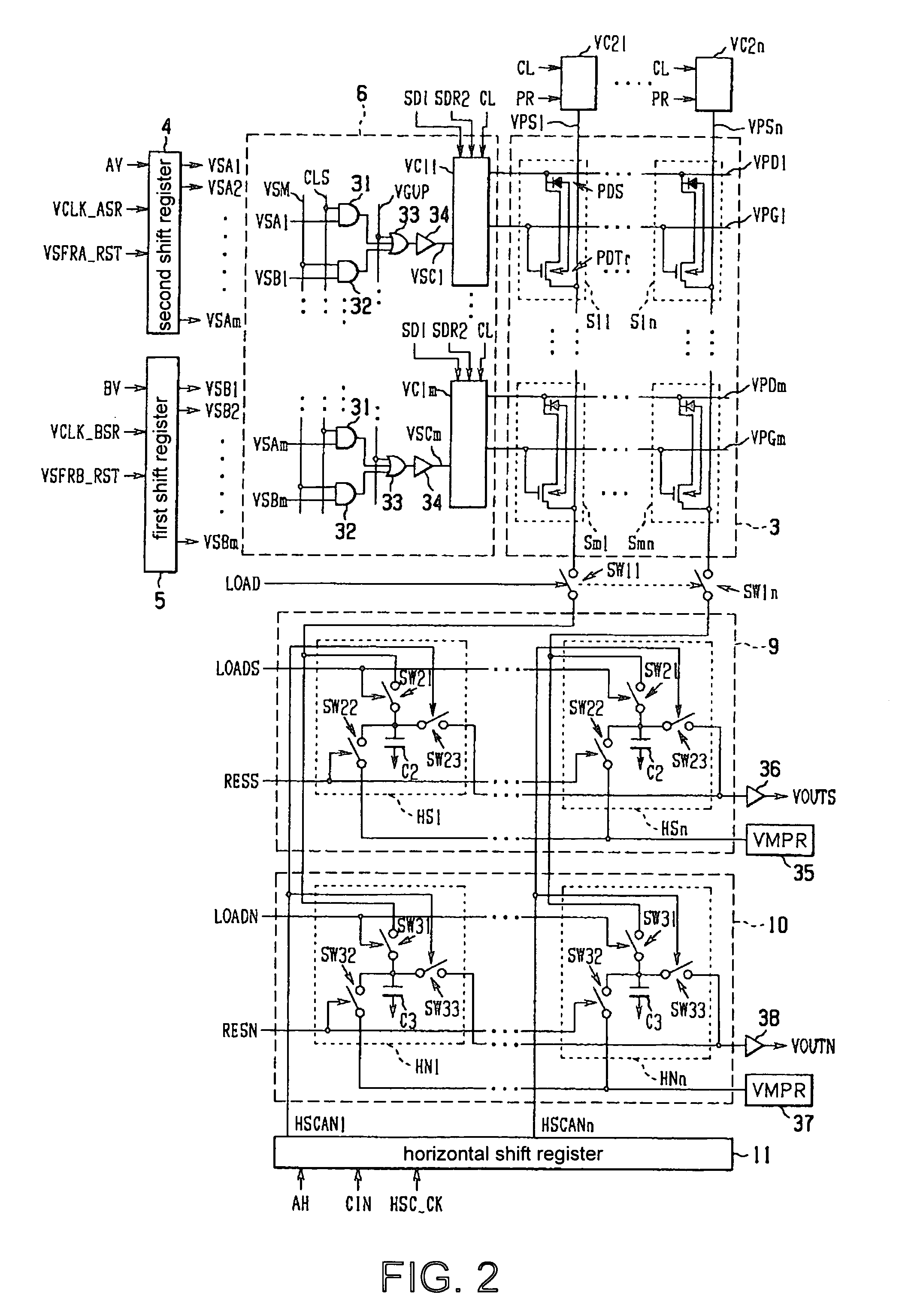
[0041] The image sensor LSI 1 includes a sensor cell array 3, a second shift register 4, a first shift register 5 and a vertical drive circuit 6 and a booster 7, a regulat...


PUM


Abstract

An image processing device is provided. The image processing device includes a first shift register connected to a line for reading out an image signal that selects a line where a signal in response to carriers accumulated in an accumulation state for generating carriers in the photo diode in response to received light is read out, regarding each line of the matrix by scanning a plurality of lines in a direction that is perpendicular to each line of a matrix and is designated, a second shift register connected to a line for clearing an image signal that selects a line for clearing an image signal where the residual carriers in the solid-state image-pickup element are discharged from the solid-state image-pickup element, and an output circuit that outputs a reset signal to the first shift register when a direction of scanning lines of the matrix is changed.

Description

RELATED APPLICATIONS [0001] Japanese Patent Application No. 2003-013606 filed on Jan. 22, 2003, is hereby incorporated by reference in its entirety. BACKGROUND OF THE INVENTION [0002] 1. Technical Field of the Invention [0003] The present invention relates to an image processing device, an image processing method and a solid-state image-pickup device. In particular, the invention relates to an image processing device that reads an image signal from a matrix type solid-state image-pickup element and an image processing method and a solid-state image-pickup device thereof. [0004] 2. Description of the Related Art [0005] A semiconductor image sensor is used for various kinds of image input devices. Recently, of such semiconductor image sensors, a MOS solid-state image-pickup device with a threshold voltage modulation system attracts attention since it provides high image quality attained by a CCD (charged coupled device) with low power consumption by a CMOS and restrains deterioration ...

Claims


Application Information

Patent Timeline
IPC IPC(8): H04N1/028H04N3/14H04N5/335H04N5/341H04N5/353H04N5/369H04N5/372H04N5/374
CPCH04N5/361H04N5/353H04N25/53H04N25/63
Inventor KANAI, MASAHIRO
Owner ADVANCED INTERCONNECT SYST LTD
Why Eureka
Try Eureka