ESD protection structure and device utilizing the same

a protection structure and electrostatic discharge technology, applied in the direction of circuit electrostatic discharge protection, hermetically sealed casings, cabinet/drawer, etc., can solve the problems of increasing the cost of the device, increasing the complexity of the electronic components, reducing the tolerance for electromagnetic interference (emi) and electrostatic discharge (esd), etc., and achieving the effect of reducing the manufacturing cos

Active Publication Date: 2005-04-28
ASUSTEK COMPUTER INC
View PDF15 Cites 20 Cited by
  • Summary
  • Abstract
  • Description
  • Claims
  • Application Information

AI Technical Summary

Benefits of technology

[0008] Accordingly, an object of the invention is to provide a simple ESD protection structure for a PCB, providing r...

Problems solved by technology

As technology improves, electronic components become more and more complicated reducing the tolerance for electromagnetic interference (EMI) and electrostatic discharge (ESD).
Gaps between controls and the housing of the device, considerable electrostatic charges carried by users, which can enter ...

Method used


Image

  • ESD protection structure and device utilizing the same
  • ESD protection structure and device utilizing the same
  • ESD protection structure and device utilizing the same

Examples


Embodiment Construction

[0018] In order to distinguish the differences between the ESD protection structure of the present invention and a conventional ESD protection circuit, the electronic device disclosed in this embodiment is, without intending to limit the disclose thereto, a CD drive.

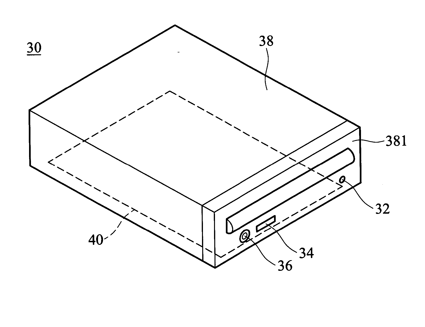
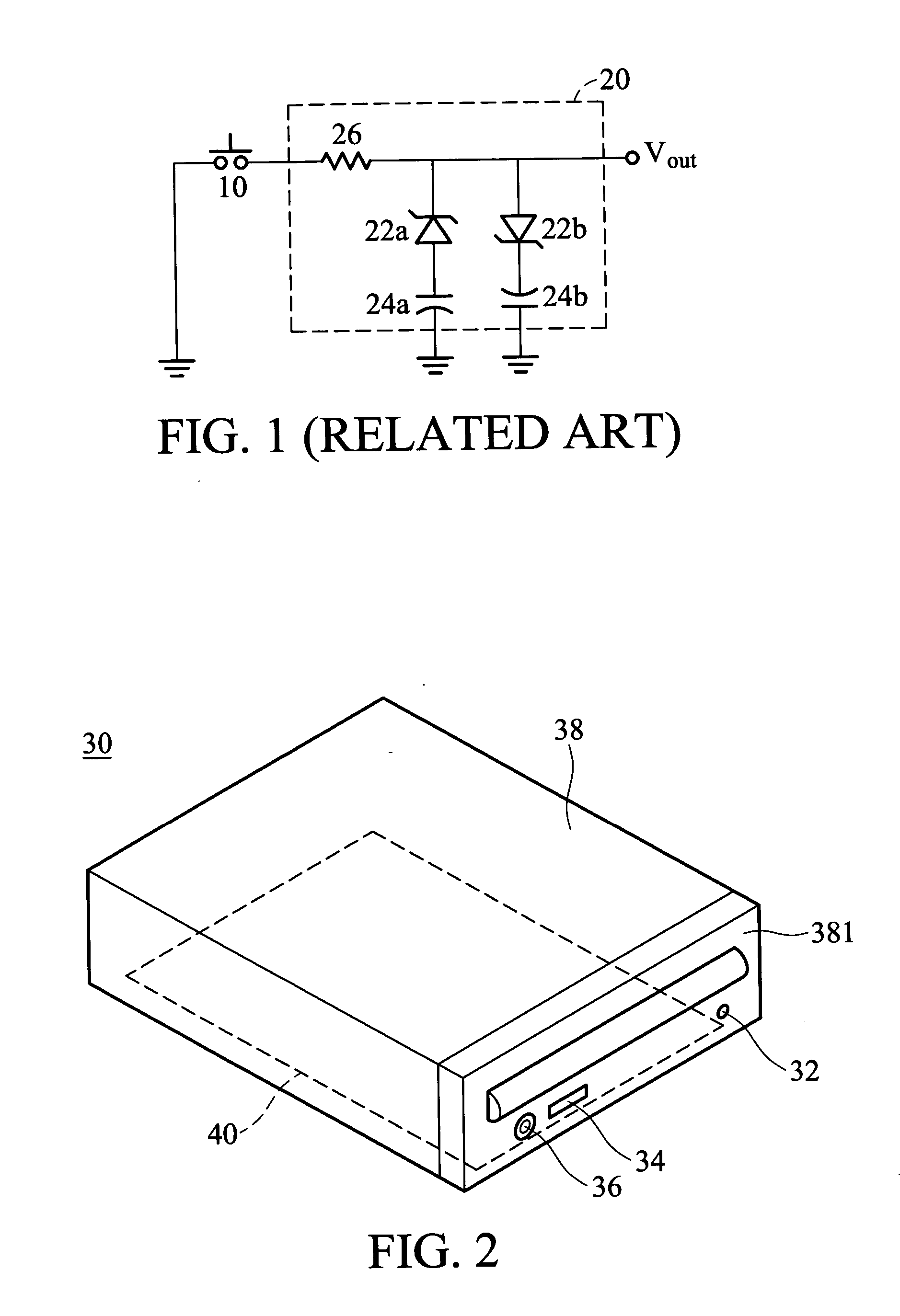
[0019]FIG. 2 shows a CD drive 30 with the ESD protection structure of the invention. In FIG. 2, the CD drive comprises a housing 38, PCB 40 and faceplate 381. The PCB 40 is disposed on the bottom surface of the housing 38. An eject control 32, volume control 34 and audio output connection 36 are disposed on the faceplate 381 and electrically connected to the PCB 40.

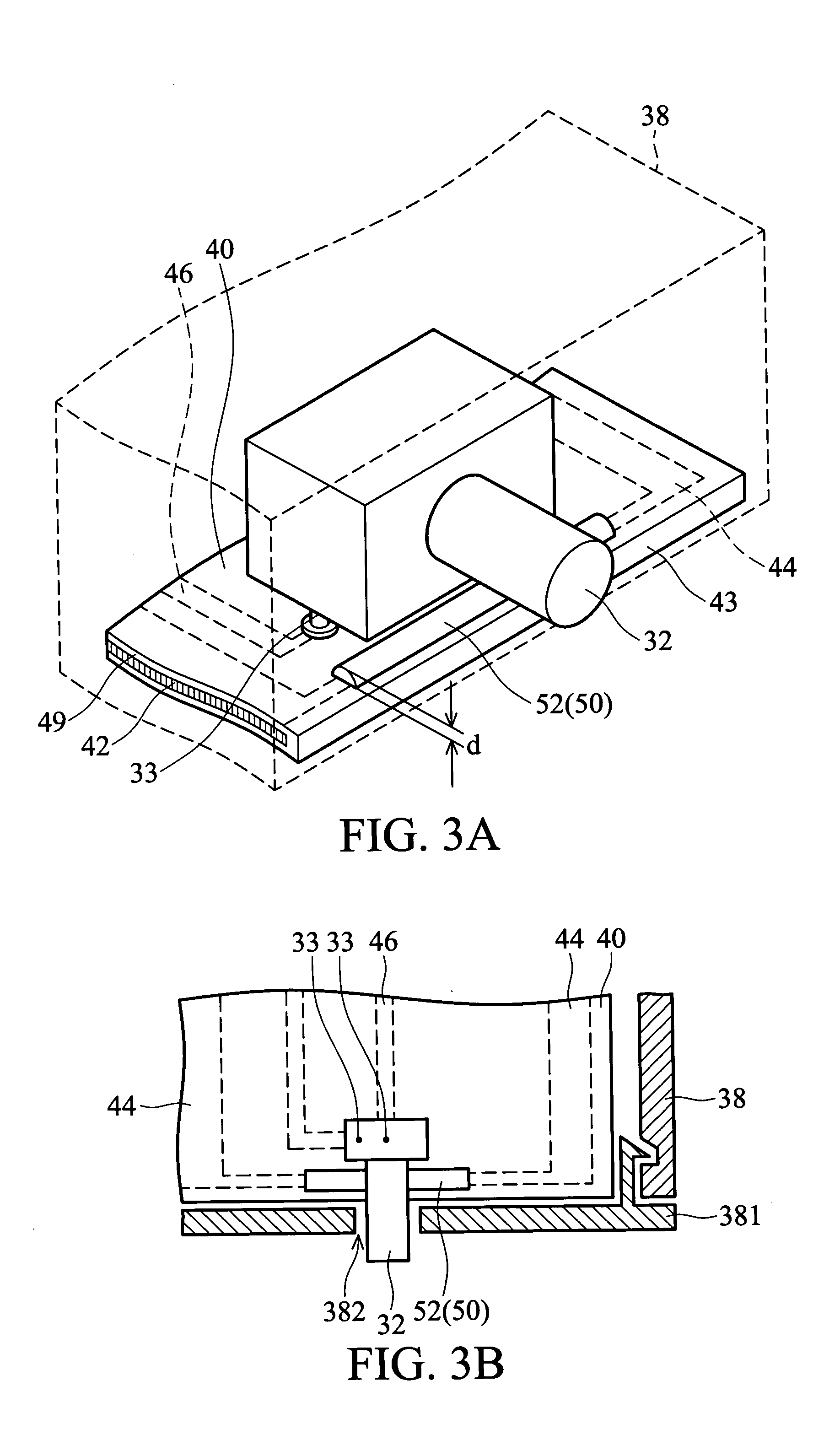
[0020]FIG. 3A is an enlarged schematic view of the CD drive near the eject control in FIG. 2. For clarity, the housing 38 of the CD drive is shown by a dashed line. FIG. 3B is a top view of FIG. 3A. The eject control 32 is connected to the PCB 40 near the front edge 43 and the faceplate 381 through two pins 33. Because the eject control 32 protrudes from the...


PUM


Abstract

An electronic device utilizing an electrostatic discharge (ESD) protection structure. The electronic device comprises a housing and a printed circuit board (PCB) with an ESD protection structure disposed thereon. The PCB has at least one metal layer with a ground circuit and a functional circuit. The ground circuit includes at least one device-protecting area near the edge of the PCB and exposed on the surface thereof. The device-protecting area is covered by a thick conductive layer, and electric components are disposed nearby, such that static electricity can be transferred to ground through the ground circuit of the PCB to protect the electronic device from interferences and damages.

Description

BACKGROUND OF THE INVENTION [0001] 1. Field of the Invention [0002] The present invention relates to an electrostatic discharge (ESD) protection structure, and in particular to an electronic device or a printed circuit board with a simplified ESD protection structure. [0003] 2. Description of the Related Art [0004] As technology improves, electronic components become more and more complicated reducing the tolerance for electromagnetic interference (EMI) and electrostatic discharge (ESD). It is therefore conventional electronic devices require additional ESD protection circuits to protect important chips or other electronic components therein. [0005] In most electronic devices, operating controls connect to specific pins of a chip to enable specific functions, such as controls for a CD drive or function keys of a mobile phone. Gaps between controls and the housing of the device, considerable electrostatic charges carried by users, which can enter circuits through air or direct contra...

Claims


Application Information

Patent Timeline
IPC IPC(8): G11B33/14H01L23/60H02H3/22H05K1/02H05K3/24H05K5/00H05K5/04H05K5/06H05K9/00
CPCG11B33/1493H05K1/0259H05K3/244H05K2201/10446H05K9/0067H05K2201/09354H05K2201/09736H05K9/0039
Inventor SU, PO-CHANGCHEN, PO-HSUN
Owner ASUSTEK COMPUTER INC
Why Eureka
Try Eureka