Semiconductor device having input/output sense amplifier for multiple sampling

a technology of sensing amplifier and semiconductor device, which is applied in the direction of information storage, static storage, digital storage, etc., can solve the problems of unnecessarily increasing the margin between the column selection line csl and the frp, and the data read operation may fail, etc., to achieve stably read

Inactive Publication Date: 2005-04-28
SAMSUNG ELECTRONICS CO LTD
View PDF4 Cites 1 Cited by
  • Summary
  • Abstract
  • Description
  • Claims
  • Application Information

AI Technical Summary

Benefits of technology

[0028] The present invention provides a semiconductor device including a sense amplifier that can stably read data regardless of a change in a temperature of, a voltage applied to, or a circuit dimension of the semiconductor device.

Problems solved by technology

However, the margin may change with a power supply voltage or temperature.
If sampling is performed when the time delay between the column selection line CSL and the FRP is small and the small signal data SGIO and / SGIO are amplified to less than the sufficient amplitude, the data read operation may fail.
However, in semiconductor devices, characteristics of the sufficient margin are very sensitive to changes in a process, a power supply voltage and temperature (PVT).
In this case, if the sufficient margin is secured at a high voltage, a semiconductor device operates at a proper speed at a high voltage, but the margin between the column selection line CSL and the FRP unnecessarily increases at a low voltage.
On the other hand, if the sufficient margin is only secured at a low voltage, the semiconductor device operates at a proper speed and flawlessly reads data at a low voltage, but a sufficient time delay between the column selection line (CSL) and the FRP is not secured at a high voltage.
As a result, an error may occur in the data read operation.
However, at a high voltage, the small signal data SGIO and / SGIO are amplified to a voltage 404 that is insufficient to read data.
In this case, an error may occur in the data read operation.
Thus, if the sufficient margin is based on a small circuit dimension, the amount of time required for the data read operation unnecessarily increases in a large circuit dimension.
Furthermore, if the sufficient margin is based on a large circuit dimension, an error may occur in the data read operation in a short circuit dimension.

Method used


Image

  • Semiconductor device having input/output sense amplifier for multiple sampling
  • Semiconductor device having input/output sense amplifier for multiple sampling
  • Semiconductor device having input/output sense amplifier for multiple sampling

Examples


Embodiment Construction

[0051] The present invention will now be described more fully with reference to the accompanying drawings, in which exemplary embodiments of the invention are shown. Throughout the drawings, like reference numerals are used to refer to like elements.

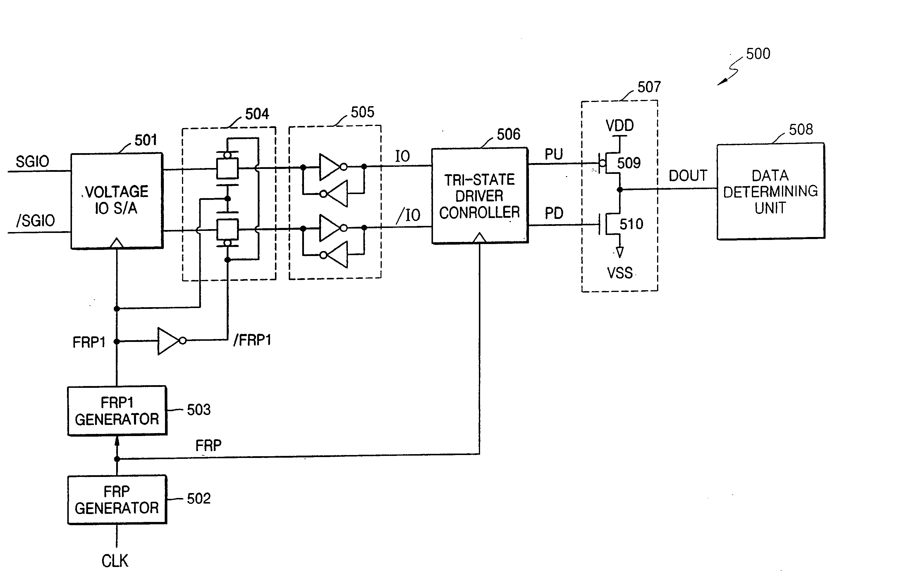
[0052]FIG. 5 illustrates a data output circuit 500 of a semiconductor device according to a first exemplary embodiment of the present invention. The data output circuit 500 shown in FIG. 5 is a type of wave pipeline processor. As the operating speed of semiconductor devices increases, a column address strobe (CAS) latency increases. To implement a long CAS latency between 5 and 6 in a semiconductor device that operates at a high speed, a data output circuit that is a type of wave pipeline processor is widely used.

[0053] Referring to FIG. 5, the data output circuit 500 includes a voltage input / output (IO) sense amplifier (S / A) 501, a first read signal (FRP) generator 502, a second read signal (FRP1) generator 503, a transmission circuit...


PUM


Abstract

Provided is a semiconductor device that is insensitive to a change in a power supply voltage, inconsistencies in a manufacturing process, and a change in temperature and provides for a rapid read data operation. The semiconductor device includes a first read signal generator, a second read signal generator, and a voltage input/output sense amplifier. The first read signal generator generates a first read signal for sampling data in response to an enable signal of a column selection line. The second read signal generator generates a second read signal including a plurality of pulses during an enabling period of the first read signal in response to the first read signal. The voltage input/output sense amplifier receives a data value output from a memory cell, amplifies the data value in synchronization with the column selection line, and samples the data value in synchronization with enabling signals of the second read signal.

Description

CROSS REFERENCE TO RELATED APPLICATION [0001] This application claims the priority of Korean Patent Application No. 2003-75633, filed on Oct. 28, 2003, in the Korean Intellectual Property Office, the disclosure of which is hereby incorporated by reference in its entirety. BACKGROUND OF THE INVENTION [0002] 1. Field of the Invention [0003] The present invention relates to a semiconductor device, and more particularly, to a semiconductor device that is insensitive to a change in a voltage, circuit dimension or temperature, and provides for a rapid read data operation. [0004] 2. Description of the Related Art [0005] With the demand for semiconductor devices with increased speed, clock frequencies of the semiconductor devices increase and time intervals between signals decrease. [0006] Also, as the amount of time necessary for data read and write operations decreases, more accurate data read and write operations are required. [0007] In particular, in the case of semiconductor devices, a...

Claims


Application Information

Patent Timeline
Patent Type & Authority Applications(United States)
IPC IPC(8): G11C11/409G11C7/06G11C7/10
CPCG11C7/04G11C7/062G11C7/1087G11C7/1057G11C7/1066G11C7/1051G11C7/06
Inventor LIM, KYU-NAM
Owner SAMSUNG ELECTRONICS CO LTD
Why Eureka
Try Eureka