Method for fabricating CMOS image sensor protecting low temperature oxide delamination

a technology of cmos and image sensors, applied in the field of method for fabricating a complementary metal oxide semiconductor (cmos) image sensor, can solve the problems of limiting the effect of these efforts, and drastically degrading the yield of probes

Active Publication Date: 2005-04-28
INTELLECTUAL VENTURES II
View PDF2 Cites 84 Cited by
  • Summary
  • Abstract
  • Description
  • Claims
  • Application Information

AI Technical Summary

Benefits of technology

[0013] It is, therefore, an object of the present invention to provide a method for fabricating a complementary metal oxide semiconductor (CMOS) image sensor capable of protecting a low temperature oxide (LTO) layer from a delamination phenomenon.

Problems solved by technology

However, since the logic circuit part is indispensable, there is a limit to what these efforts can achieve.
If the LTO crack penetrates through the pixel, a serious defect is generated to an image, thereby drastically degrading a yield of probe.

Method used


Image

  • Method for fabricating CMOS image sensor protecting low temperature oxide delamination
  • Method for fabricating CMOS image sensor protecting low temperature oxide delamination
  • Method for fabricating CMOS image sensor protecting low temperature oxide delamination

Examples


Embodiment Construction

[0025] Hereinafter, detailed descriptions on preferred embodiments of the present invention will be provided with reference to the accompanying drawings.

[0026]FIGS. 2A to 2E are cross-sectional views illustrating fabricating processes of a complementary metal oxide semiconductor (CMOS) image sensor in accordance with a preferred embodiment of the present invention. Herein, an explanation about processes performed until a passivation layer 32 is formed is omitted since it is identical to that of a conventional method.

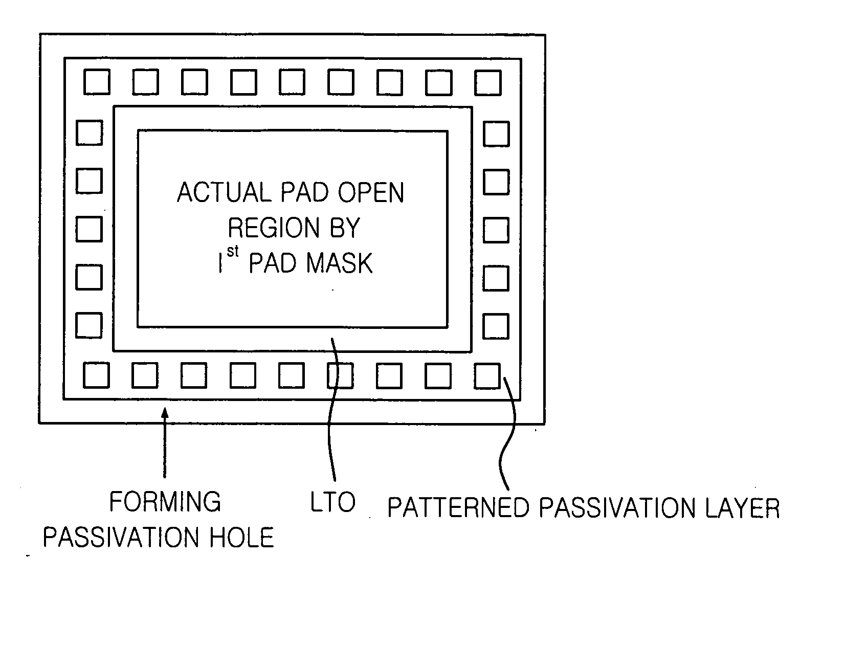
[0027] Referring to FIG. 2A, a pad metal 31 is formed on a metal inter-layer insulation layer 30 and the pad metal 31 is covered with a passivation layer 32.

[0028]FIG. 2B is a cross-sectional view illustrating the pad metal 31 exposed by selectively etching the passivation layer 32 with use of a pad mask.

[0029] Referring to FIG. 2B, a first pad etching process is performed by using a first pad mask after forming the passivation layer 32 shown in FIG. 2A.

[0030] Accor...


PUM

PropertyMeasurementUnit
temperatureaaaaaaaaaa
areaaaaaaaaaaa
opticalaaaaaaaaaa

Abstract

A method for fabricating a complementary metal oxide semiconductor image sensor is capable of protecting a low temperature oxide from delaminating a passivation layer. The method includes the steps of: forming a passivation layer on a pad metal; exposing a predetermined part of the pad metal by patterning the passivation layer using a first pad mask; forming an oxide layer on the exposed pad metal and the passivation layer formed around the pad open region; forming a color filter, a planarization layer and a microlens, sequentially; forming a low temperature oxide layer on the above structure to protect the microlens; and opening the pad metal by selectively etching the low temperature oxide layer and the oxide layer formed around the pad open region by a second pad mask.

Description

FIELD OF THE INVENTION [0001] The present invention relates to a method for fabricating a complementary metal oxide semiconductor (CMOS) image sensor; and more particularly, to a method for fabricating a CMOS image sensor capable of protecting a low temperature oxide layer from a delamination phenomenon at a pad peripheral region by performing a pad etching process twice and changing a pad layout. DESCRIPTION OF RELATED ARTS [0002] In general, an image sensor is a semiconductor device that converts an optical image into electrical signals. In a charge coupled device (CCD) is the semiconductor device that each of metal-oxide-silicon (MOS) capacitors are placed in close proximity and charge carriers are stored in or transferred between capacitors. CMOS image sensors are devices adopting a switching method for detecting output sequentially by making and using as many MOS transistors as the number of pixels based on CMOS technology that uses peripheral circuits such as control circuits ...

Claims


Application Information

Patent Timeline
Patent Type & Authority Applications(United States)
IPC IPC(8): H01L21/00H01L21/44H01L21/82H01L23/48H01L23/52H01L27/14H01L29/40H01L31/00H01L27/146H01L31/0203H04N5/335H04N5/369H04N5/374
CPCH01L27/14632H01L27/14636H01L27/14687H01L24/05H01L2924/13091H01L2224/05553H01L2924/00H01L2924/12043H01L27/146
Inventor KIM, EUN-JI
Owner INTELLECTUAL VENTURES II
Why Eureka
Try Eureka