Chemical vapor deposition unit

a technology of chemical vapor and vapor deposition unit, which is applied in the direction of chemically reactive gases, coatings, crystal growth process, etc., can solve the problems of waste of reactive gas, poor quality of semiconductor devices, and conventional chemical vapor deposition units, and achieve the effect of improving the uniformity of thickness and quality of thin films

Inactive Publication Date: 2005-05-05
SYSNEX
View PDF4 Cites 69 Cited by
  • Summary
  • Abstract
  • Description
  • Claims
  • Application Information

AI Technical Summary

Benefits of technology

[0024] Therefore, the present invention has been made in view of the above problems, and it is an object of the present invention to provide a chemical vapor deposition unit having a gas injector for injecting a single gas from a central portion thereof so as to remove by-products generated at the central region of a susceptor and to enhance the uniformity of thickness and quality of the thin film.
[0025] It is another object of the present invention to provide a chemical vapor deposition unit capable of enhancing the uniformity of thickness of the thin film by reducing the difference between densities of gases (ratio of the mixture) over the entire region of a substrate by injecting reactive gases only on the substrate.
[0026] It is yet another object of the present invention to provide a chemical vapor deposition unit capable of obtaining laminar flow of the gas over the entire region of a susceptor by removing the stagnated flow generated at regions where reaction is unnecessary, that is, a region extending from the central region of a gas injector of the chemical vapor deposition unit to the central region of the susceptor.

Problems solved by technology

Since the above-mentioned factors must be controlled, the conventional chemical vapor deposition unit has disadvantage as follows:
The by-products interfere with the deposition on the substrate (P), and as a result, the uniform thickness and quality of the thin film are deteriorated so that a poor quality of semiconductor device may be produced.
As s result, the reactive gas is wasted.
However, there is a limit to which the uniformity of the thickness and quality of the thin film can be optimized, due to the presence of by-products at the central region.
However, since the by-products are increased as the amount of gas is increased, it is almost impossible to achieve high productivity and high quality of the semiconductor.
Meanwhile, the standard deviation of the thickness is 2.11%, which is too high for the production of commercial thin films.
Since the thickness is not uniform over the whole substrate, the wavelength is also not uniform and the thickness of the thin film does not satisfy the requirements of commercial thin films.

Method used


Image

  • Chemical vapor deposition unit
  • Chemical vapor deposition unit
  • Chemical vapor deposition unit

Examples


embodiment 1

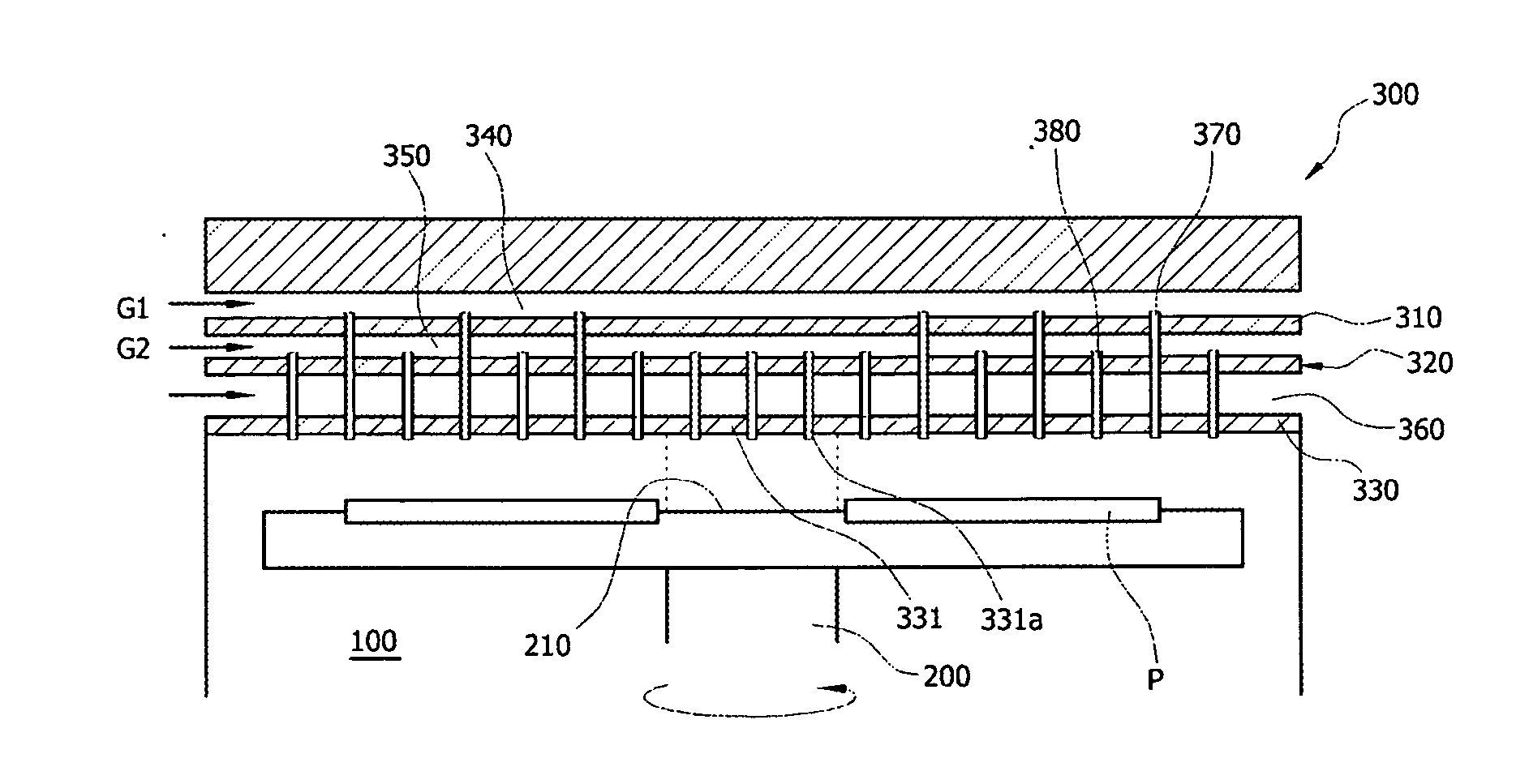
[0045] As shown in FIG. 2, a chemical vapor deposition unit according to a first embodiment of the present invention comprises a reaction chamber (100), which is isolated from the outside and kept under vacuum, a susceptor (200) installed in the reaction chamber (100), where at least one substrate (P) is placed, and a gas injector (300) for injecting different gases to form a thin film on the substrate (P) placed on the susceptor (200).

[0046] The gas injector (300) includes a first gas passage (340), a second gas passage (350), and a coolant passage (360) independently formed by partitions (310, 320, 330), disposed in turn from top to bottom as seen in the drawing, a first gas injecting pipe (370) for injecting a first gas (G1), and a second gas injecting pipe (380) for injecting a second gas (G2).

[0047] In order to allow the first and second gases (G1, G2) to be injected along the respective passages (340, 350), the tubular first and second gas injecting pipes (370, 380) have dif...

embodiment 2

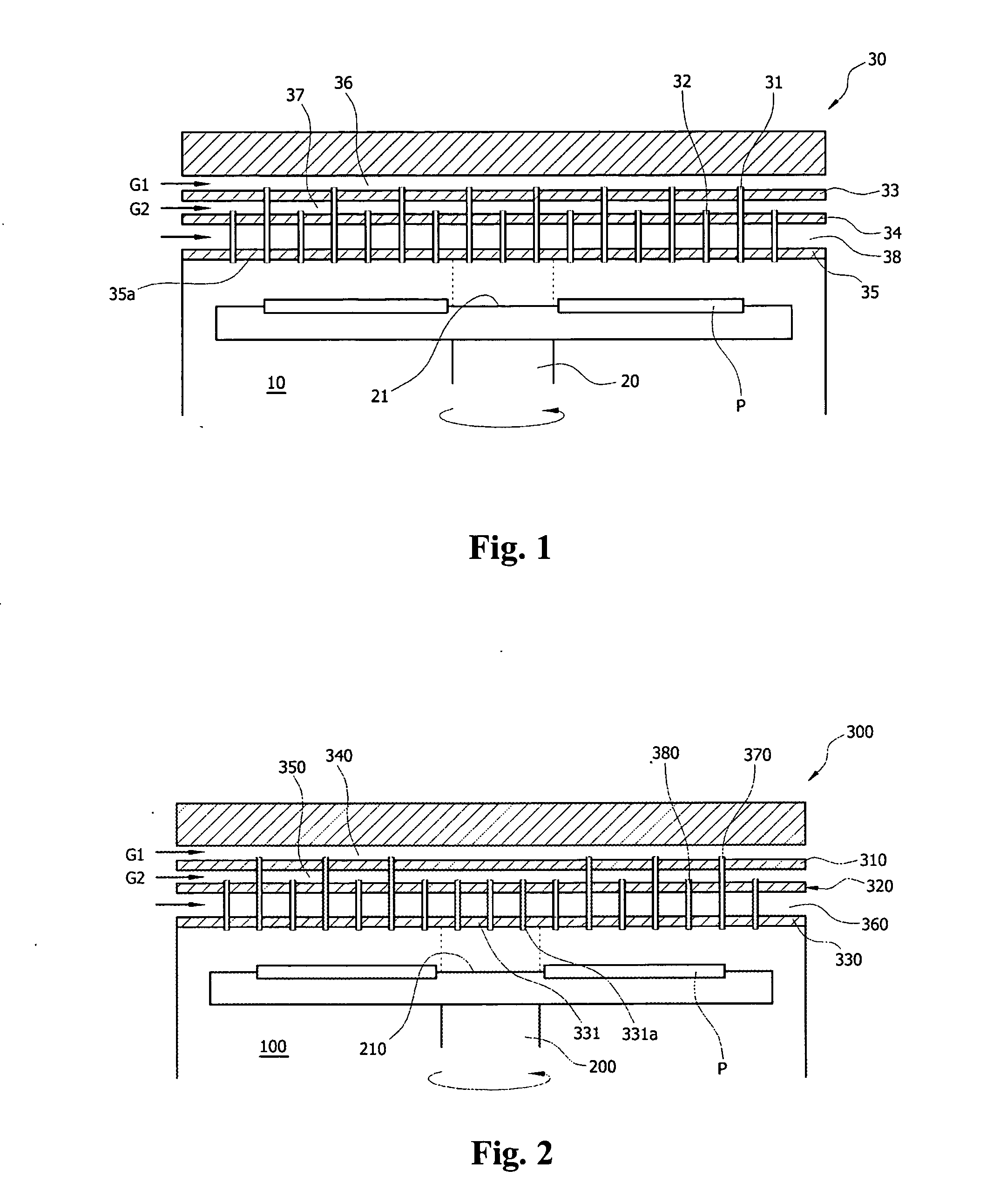
[0052] A chemical vapor deposition unit according to the second embodiment of the present invention has substantially the same structure as that of the first embodiment. However, the manufacturing process in this embodiment is simpler than that of the first embodiment, and the number of joints between the gas injecting pipes and the partitions is also reduced by reducing the number of gas injecting pipes in the central region, as compared to the gas injector shown in FIG. 2. This reduces the number of injectors that must be rejected due to inferior quality.

[0053] As shown in FIG. 3, in this embodiment, only the second gas (G2) is injected in the central region (210) of the susceptor (200) so that there is no reaction in the central region (210). By doing so, the second partition (320) is cut-out a center hole for providing central space of the second gas passage (350) through the coolant passage (360) to uniformly form the thin film on the substrate (P) disposed over the entirety o...

embodiment 3

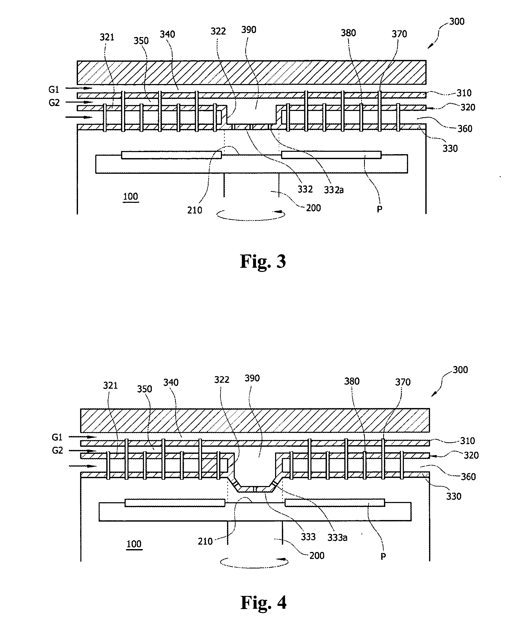
[0056] As shown in FIG. 4, a chemical vapor deposition unit according to third embodiment of the present invention is substantially the same as that of the chemical vapor deposition unit according to the second embodiment. However, the second gas injecting part (333) has protruded dome or bowl-shape downward the susceptor (200), so that the second gas (G2) injected through the injecting holes (333a) of the second gas injecting part (333) can be smoothly spread over the substrate (P).

[0057] According to third embodiment, the second gas (G2) after passing through the second gas chamber (390) is guided to flow toward the circumferential side of the susceptor (200) via the injecting hole (333), formed toward the circumferential side of the susceptor (200). Thus, the dead zone where the reaction does not take place above the susceptor (200) and the upright-bent flow are possibly minimized, so that the gas flow could be improved.


PUM

PropertyMeasurementUnit
thicknessaaaaaaaaaa
thicknessaaaaaaaaaa
thicknessaaaaaaaaaa

Abstract

A chemical vapor deposition unit is invented for forming a uniform thin film over the entire surface of a substrat by the vapor-deposition. The chemical vapor deposition unit comprises a reaction chamber isolated from the outside and kept under vacuum, a susceptor, on which at least one substrate is placed, installed in the reaction chamber such that it can rotate, and an injector, including independently formed first and second gas passages, and first and second gas injecting pipes that communicate with the respective gas passages and respective outlets, for injecting respective first and second gases onto the susceptor, the injector injecting the different gases independently. The injector further comprises a gas injecting part for communicating with the second gas passage so that only the second gas, which is a non-reactive carrier gas, is injected in a central region of the susceptor.

Description

BACKGROUND OF THE INVENTION [0001] 1. Field of the Invention [0002] The present invention relates to a chemical vapor deposition unit, and more particularly to a chemical vapor deposition unit for forming a uniform thin film over the entire surface of a substrate by providing a smooth flow of various kinds of gases to deposit a thin film on a substrate. [0003] 2. Description of the Related Art [0004] Generally, semiconductors are manufactured by the process of constructing electric circuits, repeatedly performing a diffusion process, a photographing process, an etching process, and a thin film process on a raw material of substrate. [0005] The thin film process, among the manufacturing processes for the semiconductor, is a process of vapor-depositing a thin film on a substrate to a desired thickness. Among the vapor deposition methods, there are chemical vapor deposition, ion injection, metal vapor deposition, and the like. [0006] Metal organic chemical vapor deposition, one of the ...

Claims


Application Information

Patent Timeline
Patent Type & Authority Applications(United States)
IPC IPC(8): C23C16/44C23C16/455C23C16/458C30B25/14H01L21/00H01L21/205
CPCC23C16/45565H01L21/67017C30B25/14C23C16/45574H01L21/205
Inventor LEE, KYEONG-HAKIM, SANG-CHULJUNG, DO-ILPARK, HYUN-SOO
Owner SYSNEX
Why Eureka
Try Eureka