

Single and double-gate pseudo-fet devices for semiconductor materials evaluation
- Summary
- Abstract
- Description
- Claims
- Application Information
AI Technical Summary
Benefits of technology
Problems solved by technology
Method used
Image

Examples
Embodiment Construction
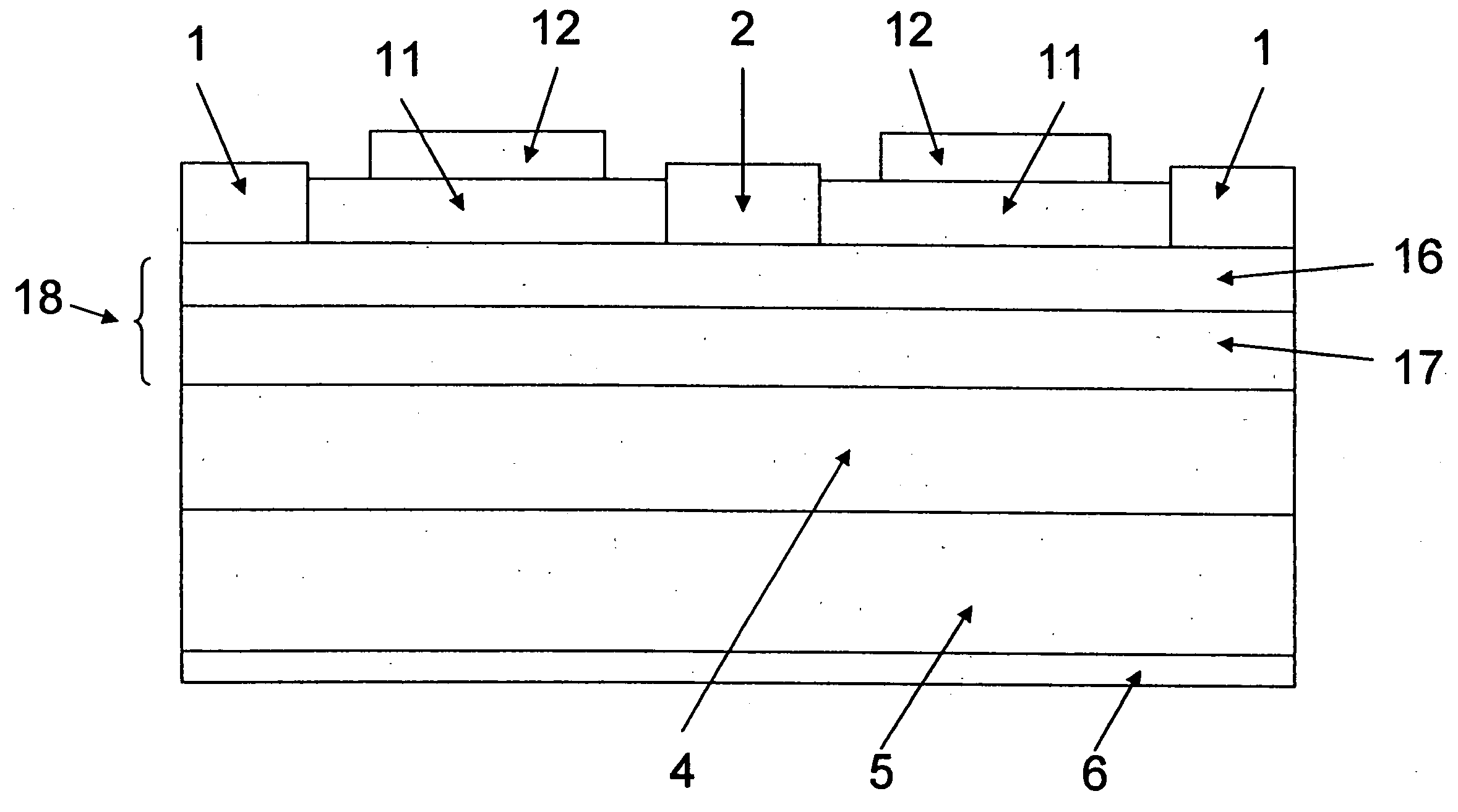
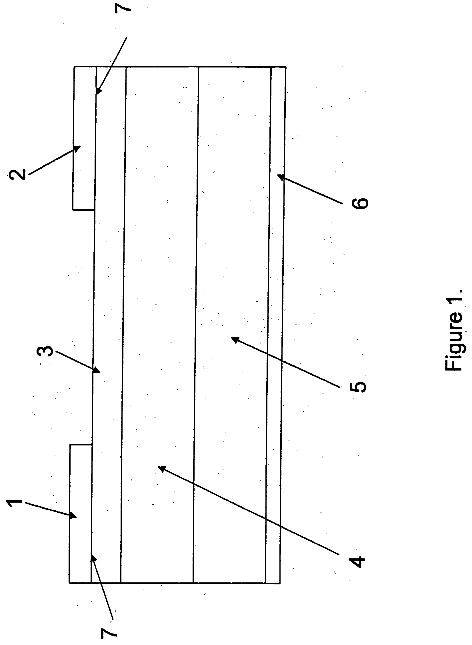
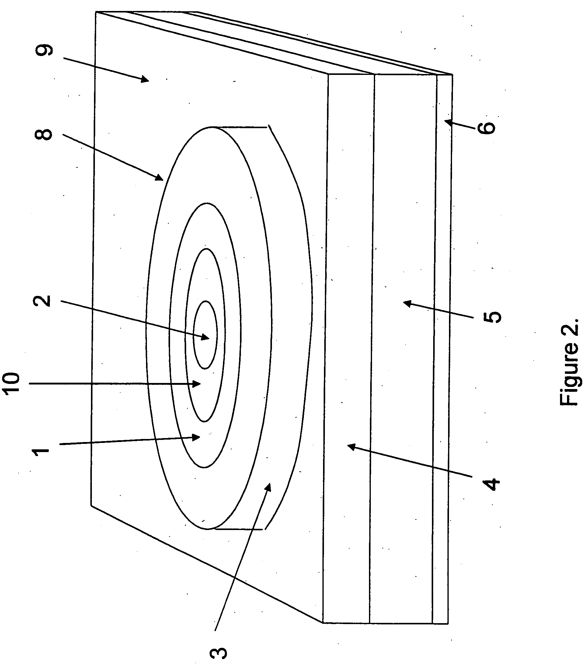
[0023]FIG. 1 shows a cross section of a single gate pseudo FET device. Silicon layer 3 resides on a buried oxide insulator 4 which resides on a Si bulk region 5. The bottom of the FET is contacted with metal 6 such as sputtered Au, Al, Cu, Cr, or other metal to provide a wide area bottom contact. (However, pseudoFET devices have been known to function satisfactorily without a bottom metal layer when the doping level and device area are sufficiently large.) Source electrode 1 and drain electrode 2 are made with Al, Er, Gd, Nd, Ti or Y, covered by Ag, Al, Au, Cr, Cu, Mg, Ni or Pt in order to provide an ohmic contact to electrons at interface 7 between the Si and electrode. Electrodes 1 and 2 may also be made with Au, Ag, Pt, Al, or Mg with or without additional covering metal to provide ohmic contact to holes at interface 7. The metal electrodes 1, 2, and 6 may be provided by evaporation or sputtering, for example. The device may be rectangular, circular, or another geometric shape. L...
PUM
 Abstract
Description
Claims
Application Information