Multi stage voltage pump circuit

a multi-stage, voltage pumping technology, applied in the direction of dc-dc conversion, power conversion systems, instruments, etc., can solve the problem of low efficiency of transferring current in conventional multi-stage voltage pumping circuits, and achieve the effect of preventing unnecessary power consumption and preventing low efficiency of transferring curren

Active Publication Date: 2005-05-05
SK HYNIX INC
View PDF4 Cites 47 Cited by
  • Summary
  • Abstract
  • Description
  • Claims
  • Application Information

AI Technical Summary

Benefits of technology

[0012] It is, therefore, an object of the present invention to provide a multi stage pumping circuit for generating a required high voltage having ability of preventing unnecessary power consumption of each stage of the multi stage pumping circuit, and, thus to prevent low efficiency of transferring current.

Problems solved by technology

Therefore, the conventional multi stage voltage pumping circuit has low efficiency of transferring current.

Method used


Image

  • Multi stage voltage pump circuit
  • Multi stage voltage pump circuit
  • Multi stage voltage pump circuit

Examples


Embodiment Construction

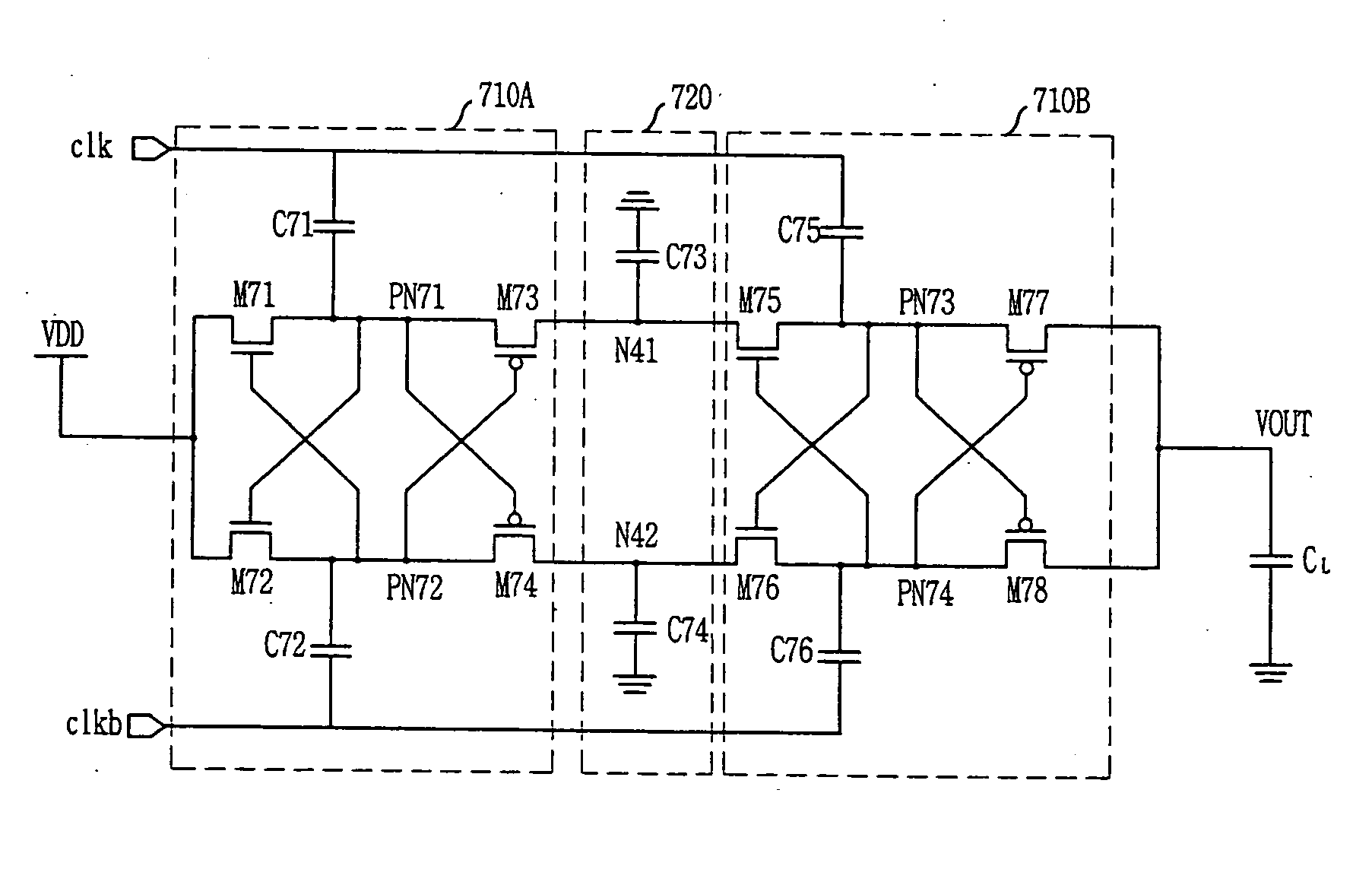
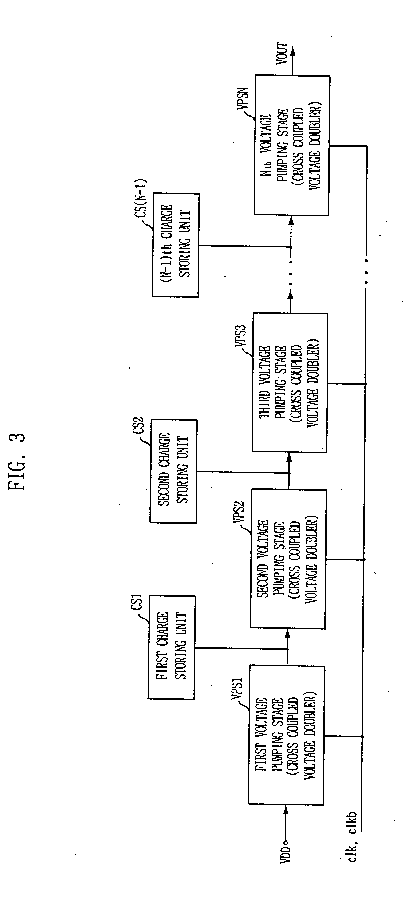
[0024] Hereinafter, a multi stage voltage pumping circuit in accordance with the present invention will be described in detail referring to the accompanying drawings.

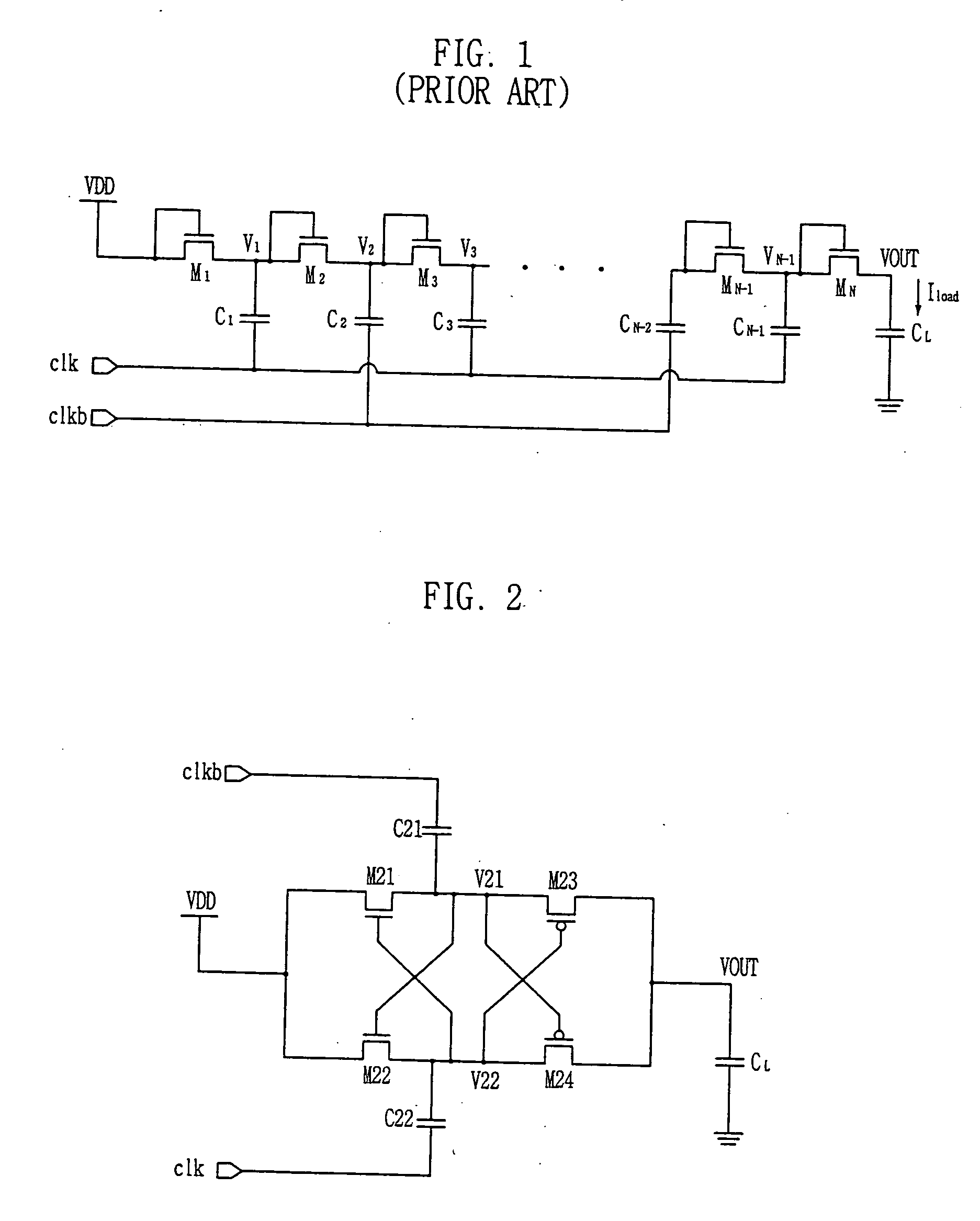
[0025]FIG. 2 is a schematic circuit diagram showing a cross coupled voltage doubler generally used for a high voltage oscillator.

[0026] An operation of the cross coupled voltage doubler is described below for explaining the principle of the present invention.

[0027] As shown, the cross coupled voltage doubler includes a first pumping capacitor C21, a second pumping capacitor C22, a first N-channel metal oxide semiconductor (NMOS) transistor pair M21 and M22 and a first P-channel metal oxide semiconductor (PMOS) transistor pair M23 and M24.

[0028] One side of the first pumping capacitor C21 receives a clock bar signal clkb and the other side is connected to a first node V21. Likewise, one side of the second pumping capacitor C22 receives a clock signal clk and the other side is connected to a second node V22.

[0029] A ...


PUM


Abstract

A multi stage voltage pumping circuit includes a plurality of voltage pumping stages each operated by a first clock signal and a second clock signal for raising a voltage level of an inputted voltage; and a plurality of charge storing means each connected to outputs of the plurality of voltage pumping stages respectively except for a last voltage pumping stage in order to store charge, wherein each of the plurality of voltage pumping stages is a cross coupled voltage doubler and an output of a previous voltage pumping stage is connected to an input of a next voltage pumping stage.

Description

FIELD OF INVENTION [0001] The present invention relates to a semiconductor device; and, more particularly, to a multi stage voltage pumping circuit capable of raising a voltage level of a power supply voltage for obtaining a high voltage. DESCRIPTION OF PRIOR ART [0002] Generally, an integrated semiconductor circuit includes a voltage pumping circuit for raising a voltage level of a power supply voltage supplied from an external circuit of the integrated semiconductor circuit, and, thus to obtain a required high voltage. For instance, the voltage pumping circuit is applied for generating a voltage required to operate a word line included in a dynamic random access memory (DRAM) or for generating a high voltage power supply in a flash memory. [0003]FIG. 1 is a schematic circuit diagram showing a conventional multi stage voltage pumping circuit. [0004] As shown, the conventional multi stage voltage pumping circuit includes a plurality of N-channel metal oxide semiconductor (NMOS) tran...

Claims


Application Information

Patent Timeline
Patent Type & Authority Applications(United States)
IPC IPC(8): G11C5/14G05F3/02H02M3/07
CPCH02M2003/077H02M3/073H02M3/077G11C5/14
Inventor LEE, DONG-UK
Owner SK HYNIX INC
Why Eureka
Try Eureka