Method for manufacturing display device and manufacturing apparatus
a display device and manufacturing apparatus technology, applied in the direction of organic semiconductor devices, semiconductor devices, instruments, etc., can solve the problems of light emitting element deterioration, reduce and display images favorably. , to achieve the effect of preventing moisture ingress, reducing manufacturing time and manufacturing costs
- Summary
- Abstract
- Description
- Claims
- Application Information
AI Technical Summary
Benefits of technology
Problems solved by technology
Method used
Image

Examples
embodiment mode 1
[Embodiment Mode 1]
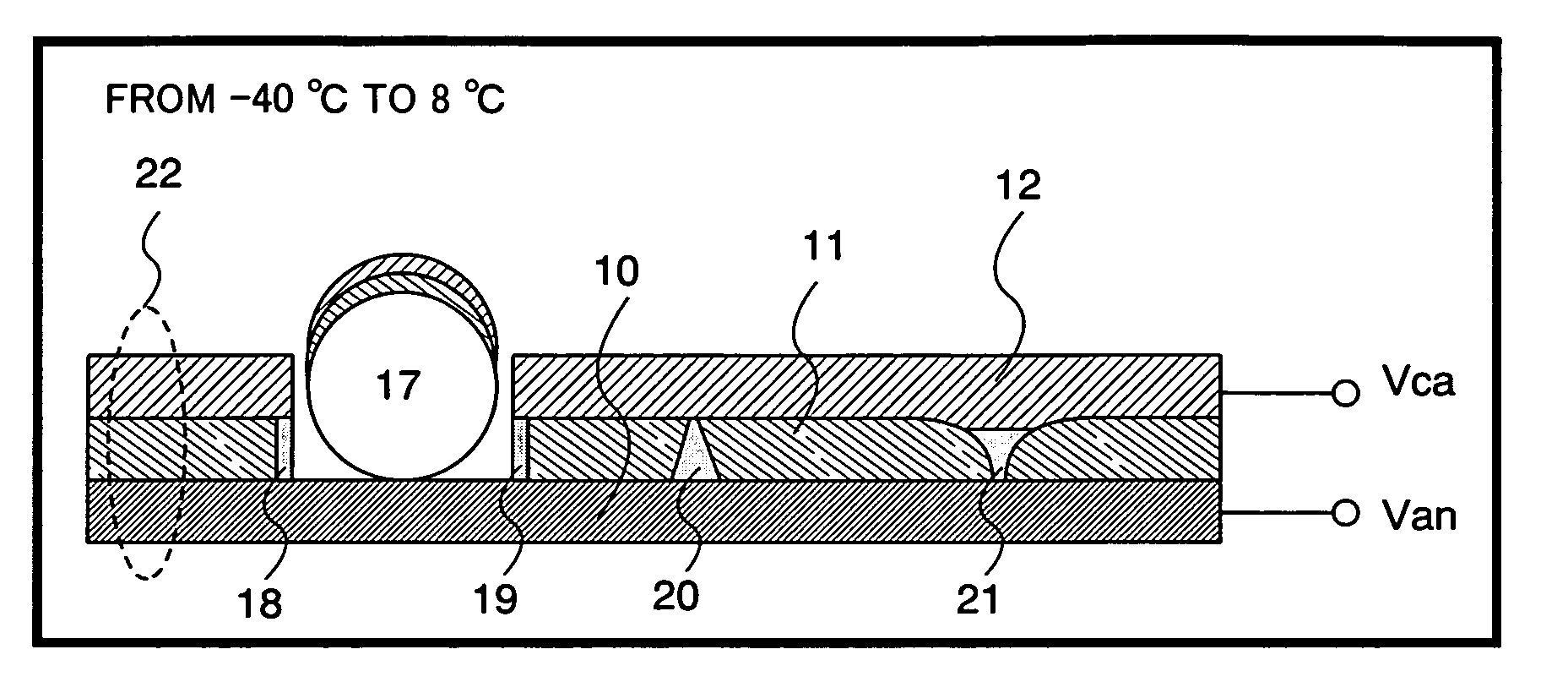
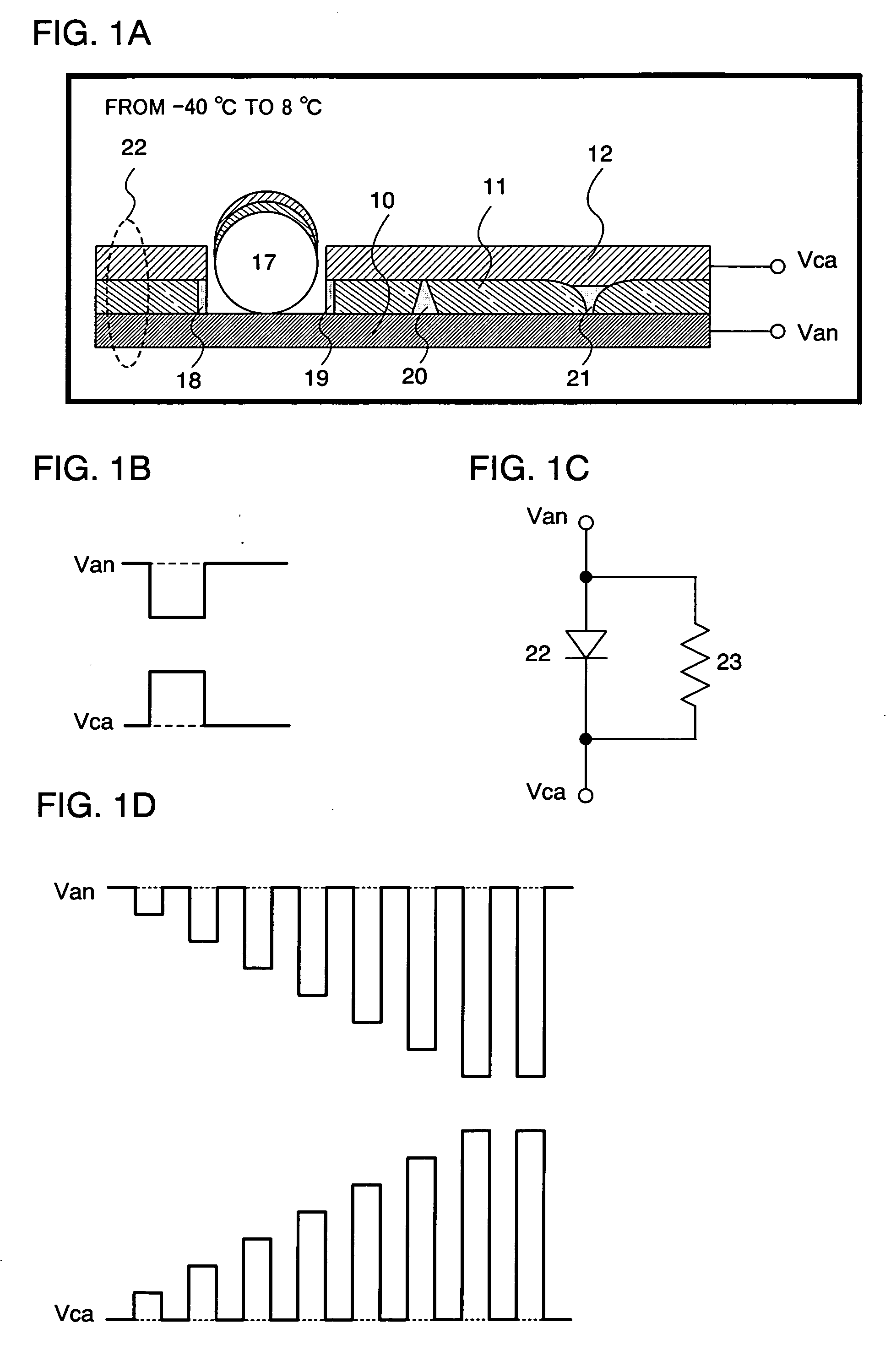
[0034] An embodiment mode of the present invention will be described with reference to FIGS. 1A to 1D. FIG. 1A shows a cross sectional structure of a light emitting element 22 in which a reverse bias voltage is applied thereto, i.e., a short-circuit portion of the light emitting element 22 is insulated. Meanwhile, FIG. 11A shows a cross sectional view of the light emitting element 22 before being applied with the reverse bias voltage. FIGS. 1B and 1D are timing charts. In FIGS. 1B and 1D, when the voltage applied to an anode 10 is Van and the voltage applied to a cathode 12 is Vca, the reverse bias voltage is applied to the anode 10 and the cathode 12 such that the voltage Vca becomes larger than the voltage Van; that is, each voltage satisfies a relational expression of Van<Vca. As depicted in FIG. 1B, the reverse bias voltage may be applied only once. Or, as depicted in FIG. 1D, the reverse bias voltage may be applied periodically so as to further increase the p...
embodiment mode 2
[Embodiment Mode 2]
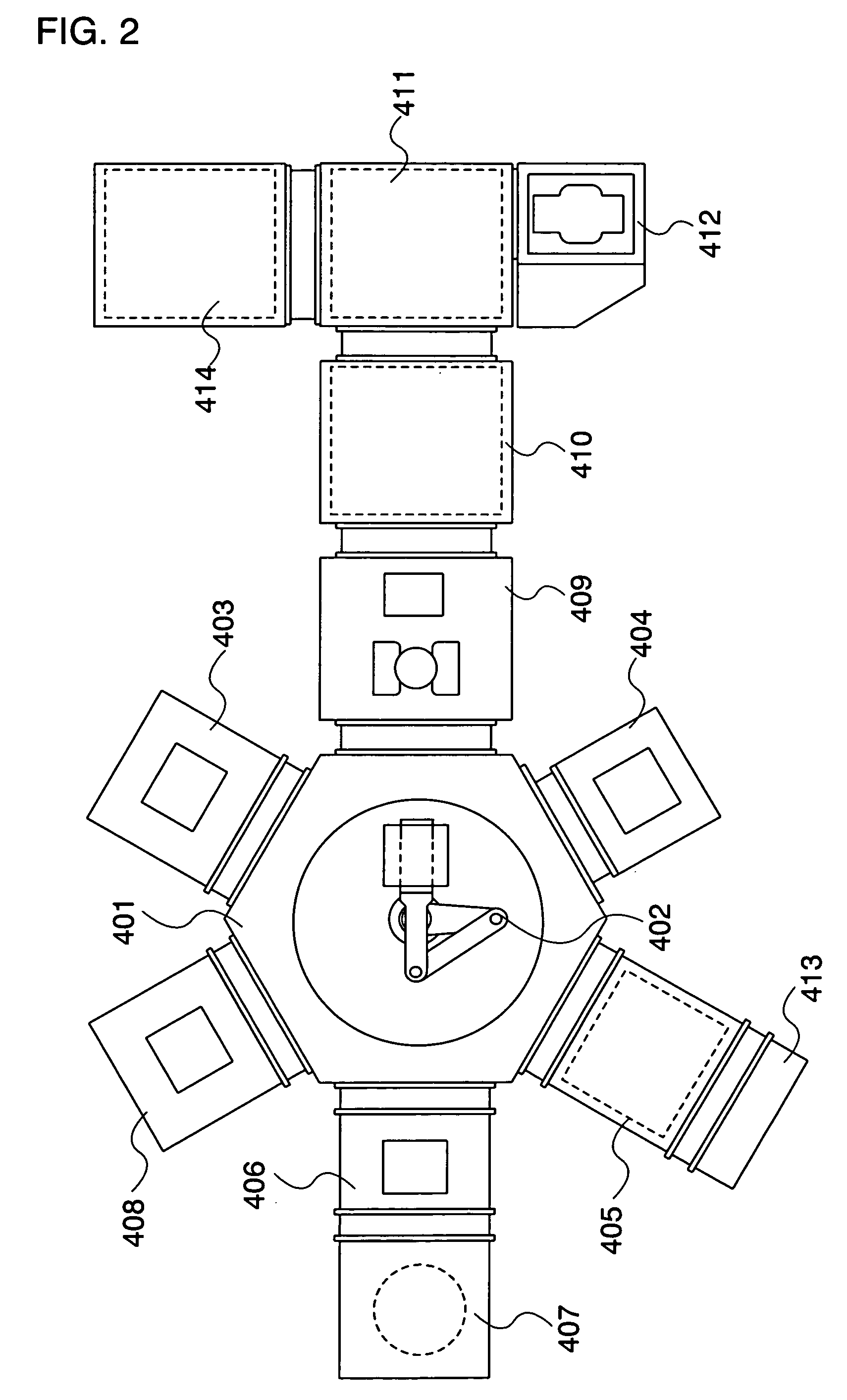
[0039] An embodiment mode of the invention will be described with reference to FIG. 2. FIG. 2 shows a manufacturing apparatus comprising one or a plurality of chambers, i.e., a multi-chamber type manufacturing apparatus. The multi-chamber type manufacturing apparatus comprises a transporting chamber 401 including a transporting mechanism 402; a loading chamber 403; a pretreatment chamber 404; a film formation chamber 405; a material changing chamber 413; a vacuum evacuation chamber 406; a film formation chamber 407; a film formation chamber 408; a sealing chamber 409; a bonding chamber 410; processing chambers 414 and 411; and a delivery chamber 412.
[0040] One or a plurality of chambers selected from the plural chambers for the multi-chamber type manufacturing apparatus is maintained at a reduced pressure. In order to reduce the pressure inside the one or the plurality of chambers, evacuation pumps such as a dry pump, a mechanical booster pump, a turbomolecular p...
embodiment 1
[Embodiment 1]
[0053] In Embodiment 1, a structure of a display device according to the present invention will be explained with reference to FIGS. 3A to 3C, and FIGS. 4A to 4D. That is, a structure of a display device, in which short-circuit portions between an anode and a cathode for a light emitting element are insulated, will be described referring to the drawings.
[0054]FIGS. 3A and 3B are cross sectional views of an active matrix light emitting display device including a light emitting element and a thin film transistor in each pixel. More specifically, FIGS. 3A and 3B show cross sectional structures of thin film transistors 201 and 202 formed over a substrate 200. These thin film transistors are top-gate thin film transistors each of which includes a polycrystalline semiconductor (polysilicon (p-Si)) in a channel portion.
[0055] Insulators 203 to 205 are formed on the thin film transistors 201 and 202. The insulators 203 to 205 are formed by using a material containing silicon...
PUM
 Abstract
Description
Claims
Application Information
 - Generate Ideas
- Intellectual Property
- Life Sciences
- Materials
- Tech Scout
- Unparalleled Data Quality
- Higher Quality Content
- 60% Fewer Hallucinations
Browse by: Latest US Patents, China's latest patents, Technical Efficacy Thesaurus, Application Domain, Technology Topic, Popular Technical Reports.
© 2025 PatSnap. All rights reserved.Legal|Privacy policy|Modern Slavery Act Transparency Statement|Sitemap|About US| Contact US: help@patsnap.com