Apparatus for single-wafer-processing type CVD

a technology of single-wafer processing and apparatus, applied in the direction of coating, metallic material coating process, chemical vapor deposition coating, etc., can solve the problems of reducing yield, contaminating semiconductor production lines, damaging semiconductor wafers, and generating particles, so as to achieve the effect of effectively preventing the deposition of unnecessary portions

Inactive Publication Date: 2005-05-12
ASM JAPAN
View PDF16 Cites 234 Cited by
  • Summary
  • Abstract
  • Description
  • Claims
  • Application Information

AI Technical Summary

Benefits of technology

[0007] From the viewpoint of the susceptor construction, which may have a multiple number of wafer lift pins and in which the holes of wafer lift pins are used for gas discharge holes, gas discharge from the susceptor can be achieved easily. Gas discharge holes are not limited to the wafer lift pin holes, holes provided in the susceptor other than the gas discharge hoes can serve as the gas discharge holes.
[0008] According to another embodiment, in the above-mentioned apparatus, gas discharge holes are provided in the susceptor and can be also provided outside a position of placing the object-to-be-processed to make gas flow out into the reaction chamber through the periphery of the object-to-be-processed during deposition. In this case, a circumference portion on the inside of the sealing means of the separation plate bottom can be disposed in such a position th

Problems solved by technology

If a metal film whose effects on these metal films or a semiconductor apparatus have not been known is deposited using a conventional CVD apparatus, contamination of semiconductor production lines is likely to be caused by metal contamination of the back side or an edge of objects-to-be-processed, lowering yield.
This method creat

Method used


Image

  • Apparatus for single-wafer-processing type CVD
  • Apparatus for single-wafer-processing type CVD
  • Apparatus for single-wafer-processing type CVD

Examples


embodiment

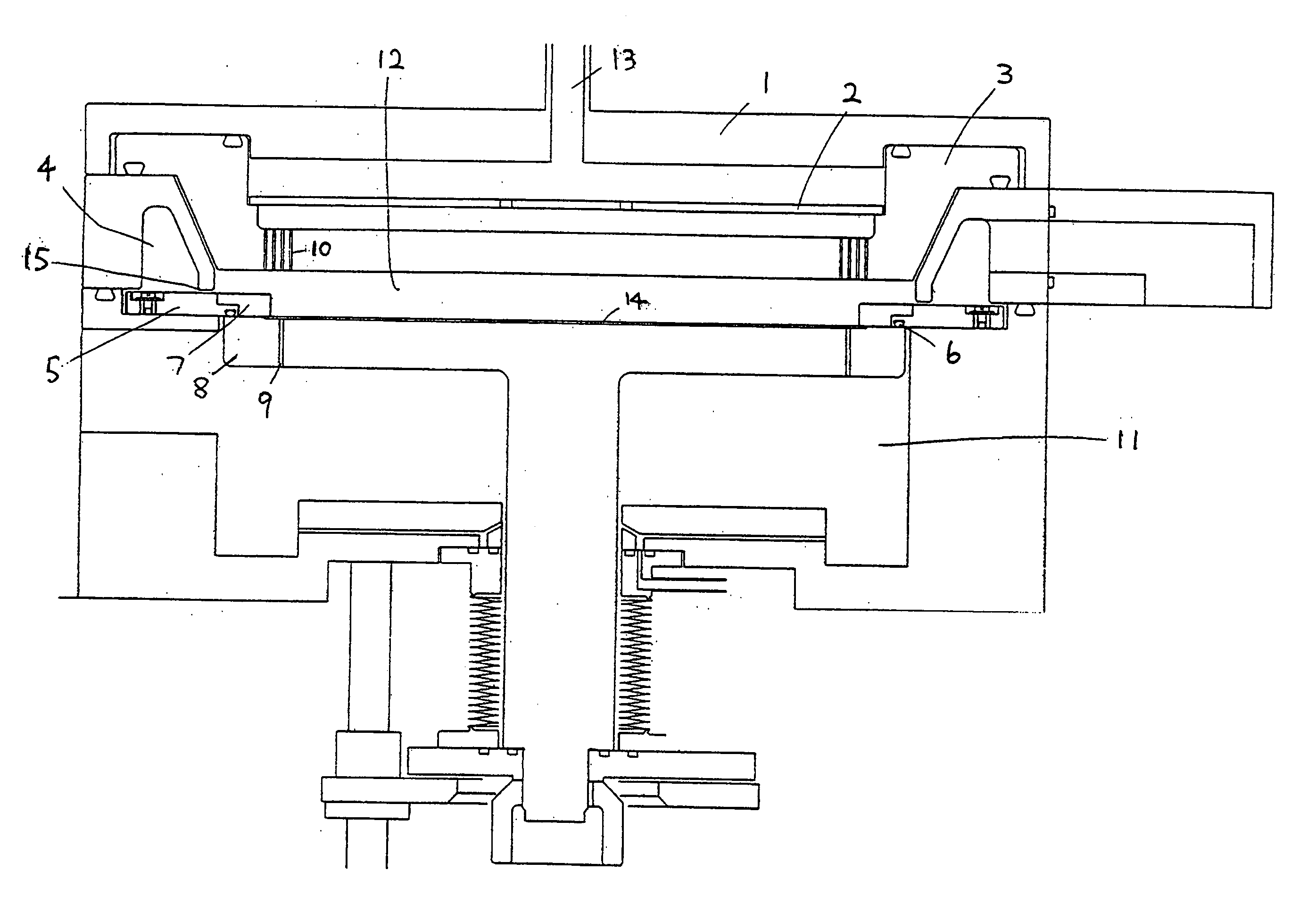
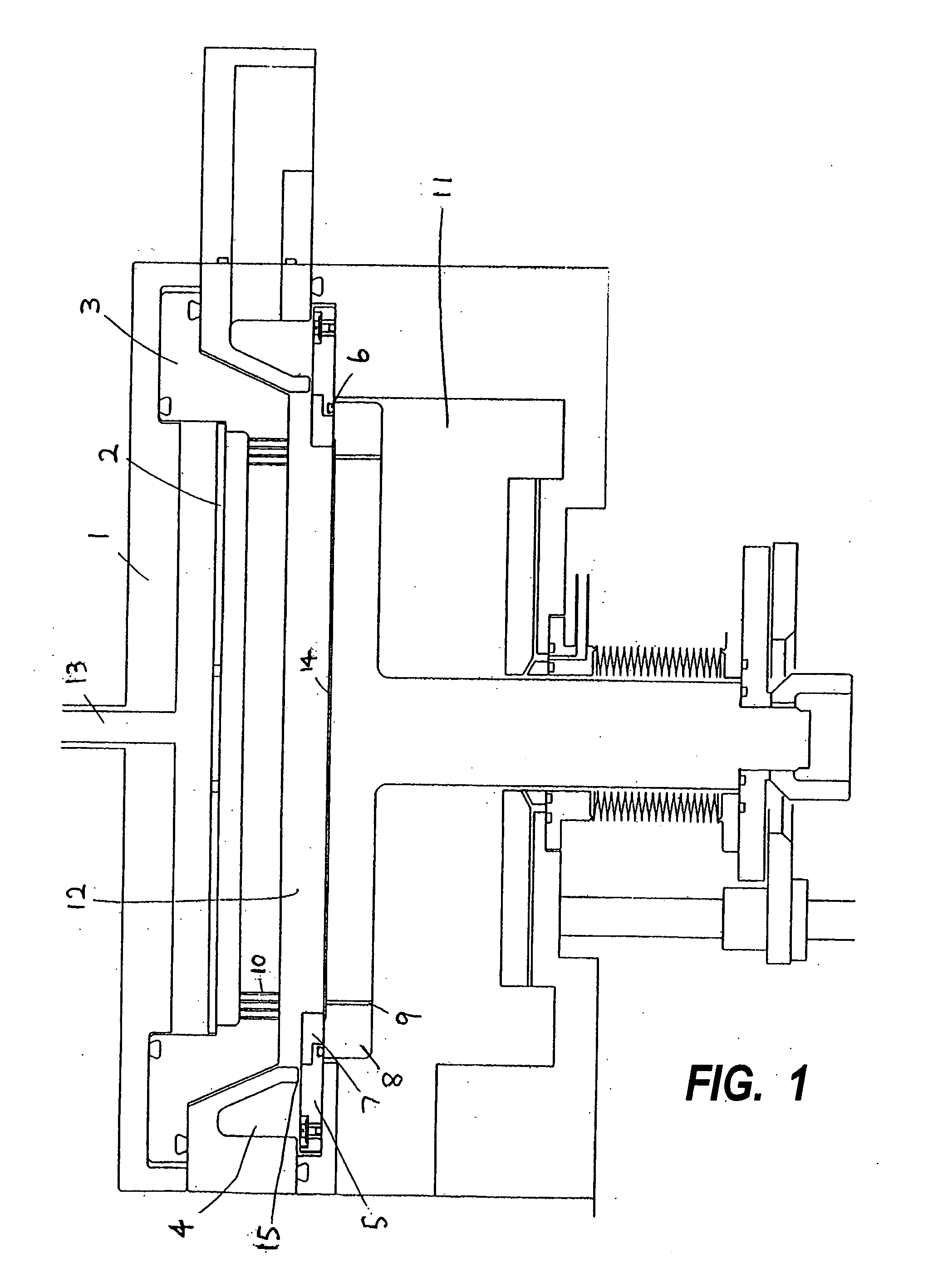
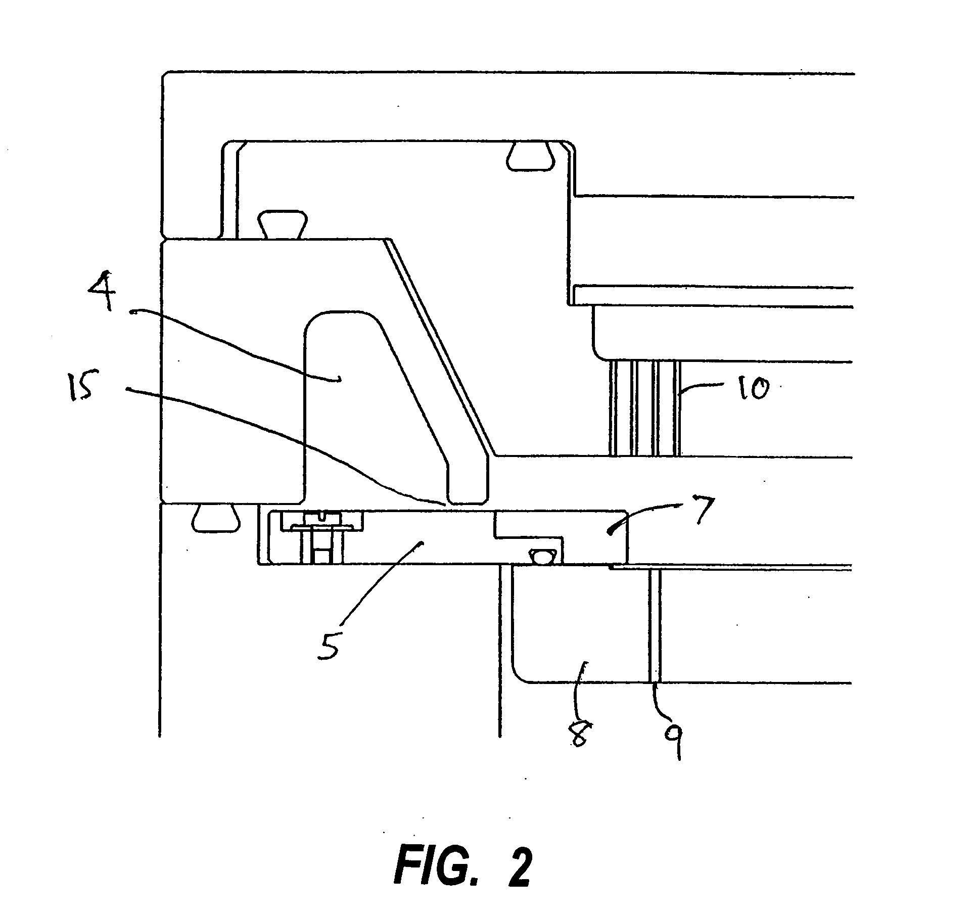
[0052] An embodiment of the present invention is described using Cu film deposition using the reactor shown in FIG. 1 as an example. After a semiconductor wafer is transferred from an evacuated load-lock chamber (not shown) to a susceptor 8, the susceptor is raised to a reaction position by a susceptor elevating means. At this time, the periphery of the susceptor is sealed by an O-ring provided at the lower portion of a separation plate 5, and the wafer-handling chamber 11, and the reaction chamber 12 are completely separated. At this time, the periphery of the wafer of 2 mm is completely covered by the guard ring 7. By supplying Ar from the wafer-handling chamber through holes 9 provided in the susceptor, deposition onto the back side and the edge of the wafer is prevented. After the susceptor is raised into the reaction chamber, 1000 sccm of inert gas is brought in from a gas inlet port 13. While the inert gas is emitted onto the wafer from holes 10 provided in the showerhead 3 a ...


PUM

PropertyMeasurementUnit
Temperatureaaaaaaaaaa
Lengthaaaaaaaaaa

Abstract

A single-wafer-processing type CVD apparatus includes: (a) a reaction chamber including: (i) a susceptor having at least one gas discharge hole to flow a gas into the reaction chamber via a back side and a periphery of the wafer into the reaction chamber; (ii) a showerhead; (iii) an exhaust duct positioned in the vicinity of the showerhead and provided circularly along an inner wall of the reaction chamber; and (iv) a circular separation plate provided coaxially with the exhaust duct to form a clearance with the bottom of the exhaust duct; and (b) a temperature-controlling apparatus for regulating the temperature of the showerhead. The separation plate has a sealing portion to seal a periphery of the susceptor and to separate the reaction chamber from a wafer-handling chamber when the susceptor rises.

Description

BACKGROUND OF THE INVENTION [0001] This is a divisional application of U.S. patent application Ser. No. 10 / 403,179 filed Mar. 28, 2003 which claims the benefit of U.S. Provisional Application No. 60 / 372,624, filed Apr. 12, 2002. The disclosure of the above applications is herein incorporated by reference in its entirety.FIELD OF THE INVENTION [0002] The present invention relates to single-wafer-processing type CVD (Chemical Vapor Deposition) which forms a thin film on a semiconductor wafer, which is an object-to-be-processed. DESCRIPTION OF THE RELATED ART [0003] Due to high integration of a semiconductor apparatus, interconnects using Cu, which has lower electrical resistance than Al interconnects which were used in the past, have come into use. Additionally, when Cu is used for interconnects, it becomes necessary to form a metal film such as TiN, TaN, etc., which had not conventionally been used before, as a barrier metal for preventing diffusion of Cu. In the present circumstance...

Claims


Application Information

Patent Timeline
IPC IPC(8): C23C16/44C23C16/455C23C16/458C23C16/54H01L21/285H01L21/3065
CPCC23C16/4409C23C16/4412C23C16/45521C23C16/54C23C16/45572C23C16/4585C23C16/4557H01L21/205
Inventor SHIMIZU, AKIRAFUKUDA, HIDEAKIKAWANO, BAIEISATO, KAZUO
Owner ASM JAPAN
Why Eureka
Try Eureka