Semiconductor device and method of manufacturing the same

a technology of semiconductor devices and semiconductors, applied in semiconductor devices, semiconductor/solid-state device details, electrical apparatus, etc., can solve problems such as manufacturing process trouble, possible defective connection,

Inactive Publication Date: 2005-05-12
AOI ELECTRONICS CO LTD
View PDF18 Cites 110 Cited by
  • Summary
  • Abstract
  • Description
  • Claims
  • Application Information

AI Technical Summary

Problems solved by technology

The particular construction gives rise to the problem that it is possible for the defective connection to take place depending on the state of the bonding.
Also, it is necessary to mount the semiconductor chips 1 one by one to the relay substrate 4 so as to make the manufacturing process troublesome.

Method used


Image

  • Semiconductor device and method of manufacturing the same
  • Semiconductor device and method of manufacturing the same
  • Semiconductor device and method of manufacturing the same

Examples


first embodiment

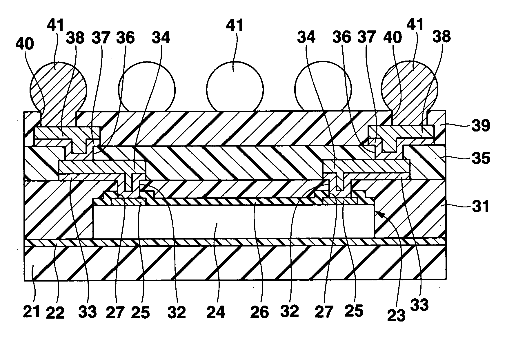
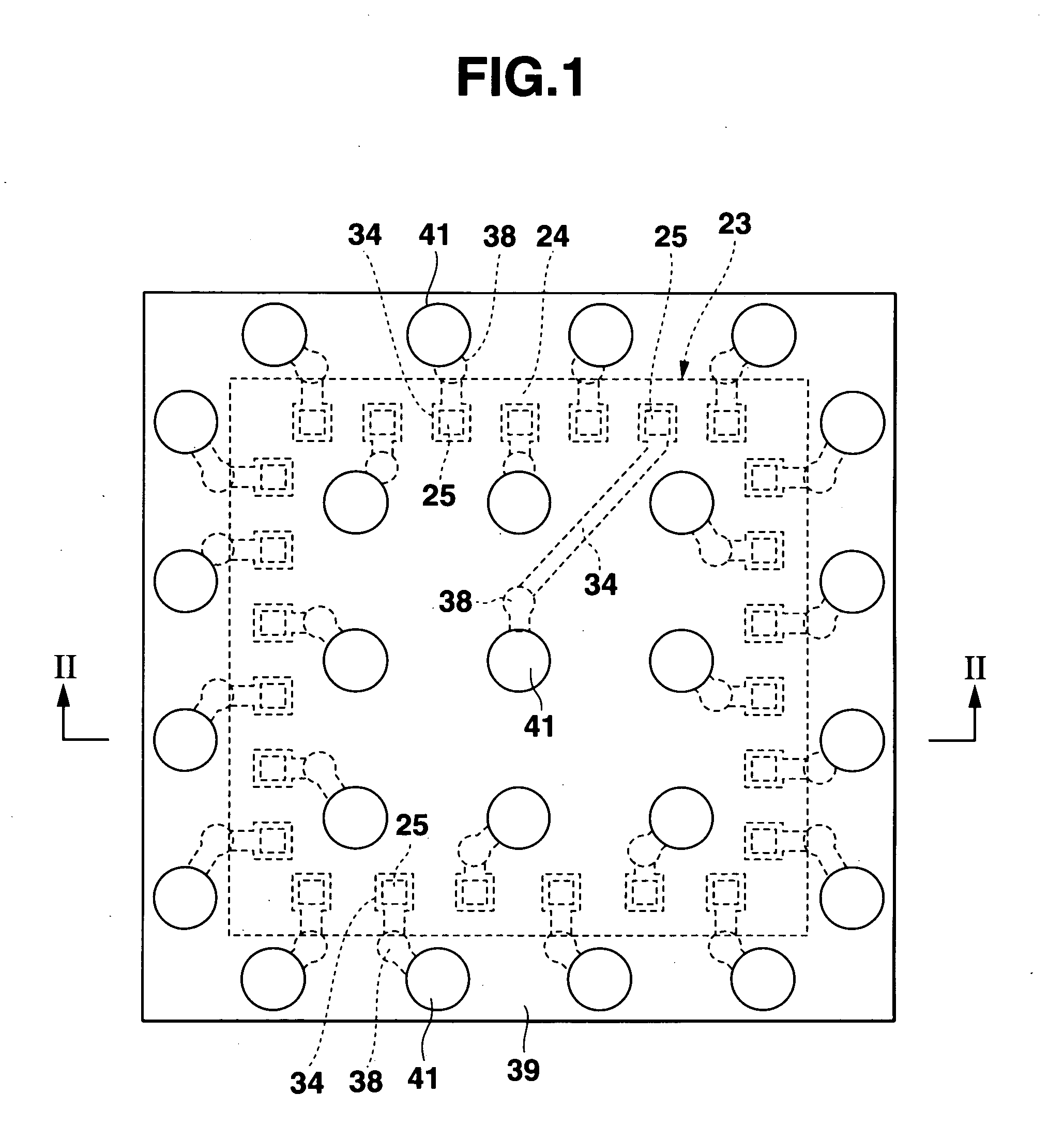
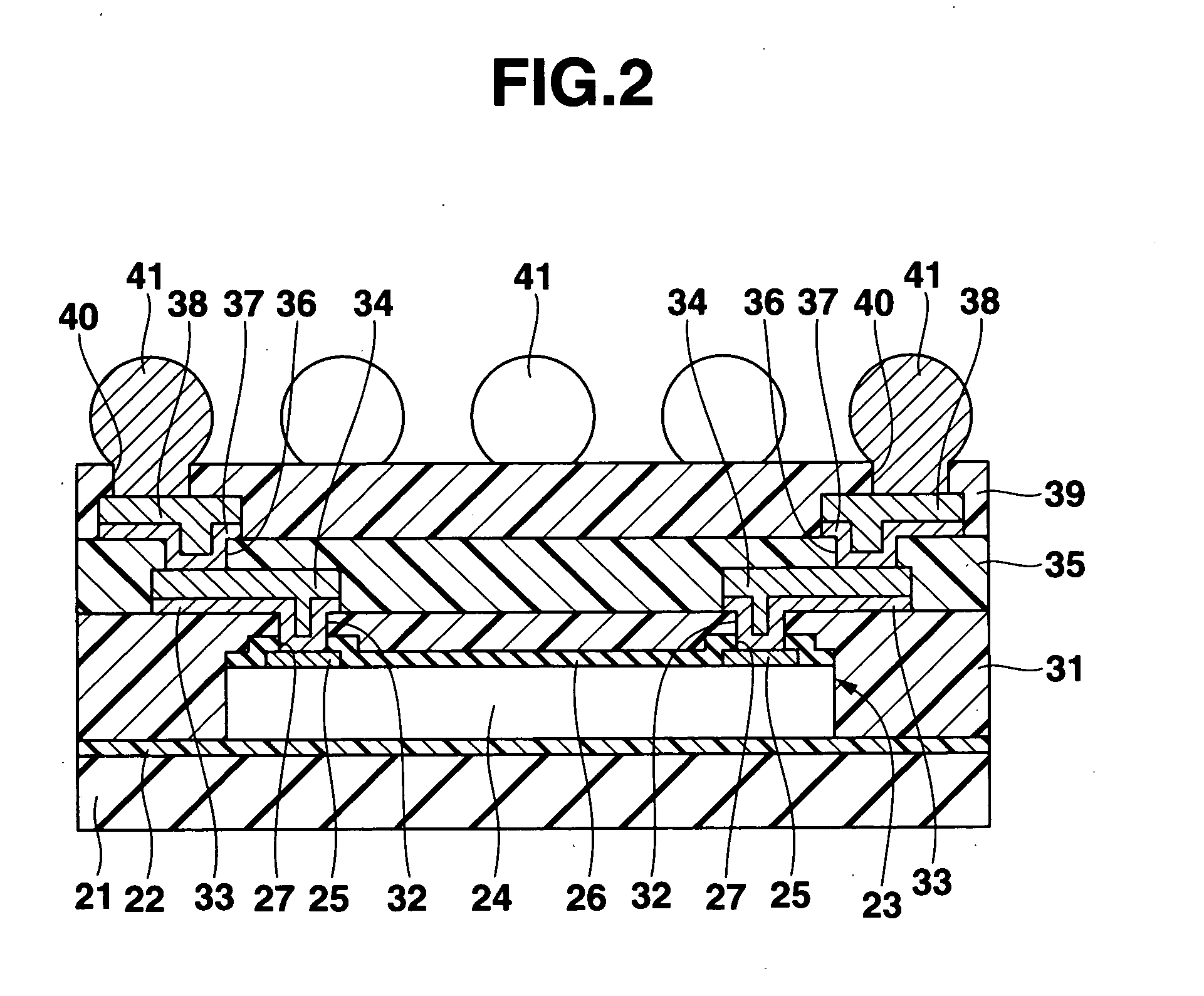
[0059]FIG. 1 is a plan view showing a semiconductor device according to a first embodiment of the present invention, and FIG. 2 is a cross sectional view along the line II-II shown in FIG. 1. In this case, FIGS. 1 and 2 are not equal to each other in the size of each member of the semiconductor device.

[0060] The semiconductor device comprises a base plate 21 having a square planar shape and made of, for example, a resin plate, a metal plate or glass plate. An adhesive layer 22 made of, for example, an adhesive, an adhesive sheet or a double-coated adhesive tape is formed on the entire upper surface of the base plate 21. The lower surface of a silicon substrate 24 of a substantially square semiconductor chip 23 sized somewhat smaller than the base plate 21 is mounted on the central portion of the upper surface of the adhesive layer 22.

[0061] The semiconductor chip 23 includes a plurality of connection pads 25 made of, for example, aluminum and mounted to the upper peripheral portio...

second embodiment

[0082]FIG. 12 is a vertical cross sectional view showing a semiconductor device according to a second embodiment of the present invention. The semiconductor device shown in FIG. 12 widely differs from the semiconductor device shown in FIG. 2 in that, in the semiconductor device shown in FIG. 12, the pad portion of the first re-wiring 34 is connected to the second underlying metal layer 37 positioned below the second re-wiring 38 via a columnar electrode 61 arranged within the open portion 36 formed in the portion of the second insulating film 35 above the pad portion.

[0083] An example of the method of manufacturing the semiconductor device shown in FIG. 12 will now be described. In this case, the manufacturing steps up to the step of peeling off the plating resist film 51 shown in FIG. 4 are equal to those for the first embodiment of the present invention described previously. Therefore, the subsequent manufacturing steps will now be described in conjunction with the second embodim...

third embodiment

[0093] Where the adhesive layer 22 is formed on only the lower surface of the silicon substrate 24 of the semiconductor chip 23 and the adhesive layer22 is bonded to a prescribed position on the upper surface of the base plate 21 in the manufacturing step shown in FIG. 3, it is possible to obtain a semiconductor device according to a third embodiment of the present invention, which is shown in FIG. 19. For forming the adhesive layer 22 on the lower surface of the silicon substrate 24 of the semiconductor chip 23, it is efficient to fix the adhesive layer 22 to the back surface of the silicon wafer having connection pads 25 and an insulating film 26 formed thereon, followed by dicing the silicon wafer so as to obtain the semiconductor chip 23 having the adhesive layer 22 formed on the back surface. Alternatively, it is possible to drip a die coating material by using, for example, a dispenser onto those regions of the base plate 21 on which the semiconductor chips 23 are to be mounte...


PUM

PropertyMeasurementUnit
thicknessaaaaaaaaaa
thicknessaaaaaaaaaa
heightaaaaaaaaaa

Abstract

A plurality of semiconductor chips (23) are bonded to an adhesive layer (22) formed on a base plate (21). Then, first to third insulating films (31, 35, 39), first and second underlying metal layers (33, 37), first and second re-wirings (34, 38), and a solder ball (41) are collectively formed for the plural semiconductor chips (23). In this case, the first and second underlying metal layers (33, 37) are formed by a sputtering method, and the first and second re-wirings (34, 38) are formed by an electroplating method. Then, a laminate structure consisting of the three insulating films (39, 35, 31), the adhesive layer (22), and the base plate (21) is cut in a region positioned between the adjacent semiconductor chips (23).

Description

TECHNICAL FIELD [0001] The present invention relates to a semiconductor device and a method of manufacturing the same, particularly, to a semiconductor device in which a rewiring is formed directly on one surface of a semiconductor chip like a chip size package (CSP) and a method of manufacturing the same. BACKGROUND ART [0002] A conventional semiconductor device called, for example, a BGA (ball grid array) includes a device in which a semiconductor chip made of, for example, an LSI is mounted in the central portion on the upper surface of a relay substrate (interposer) sized somewhat larger than the semiconductor chip, and connection terminals formed of solder balls are arranged to form a matrix on the lower surface of the relay substrate. [0003]FIG. 45 is a vertical cross sectional view exemplifying the construction of such a conventional semiconductor device. As shown in the figure, a semiconductor chip 1 includes a silicon substrate 2 and a plurality of bump electrodes 3 made of...

Claims


Application Information

Patent Timeline
Patent Type & Authority Applications(United States)
IPC IPC(8): H01L21/58H01L21/60H01L21/68H01L23/31H01L23/538H01L25/10
CPCH01L21/568H01L21/6835H01L23/3114H01L23/5389H01L24/19H01L24/97H01L25/0655H01L25/105H01L2221/68345H01L2224/24226H01L2224/2518H01L2224/97H01L2924/01002H01L2924/01013H01L2924/01029H01L2924/01032H01L2924/01033H01L2924/01075H01L2924/01078H01L2924/15173H01L2924/15174H01L2924/15311H01L2924/15331H01L2924/18161H01L2924/19041H01L2924/19042H01L2924/19043H01L2924/19105H01L2924/30107H01L2924/01006H01L24/83H01L2224/16225H01L2224/32225H01L2224/73204H01L2224/05548H01L2224/05567H01L2224/13022H01L2225/1035H01L2225/1058H01L2224/24195H01L2224/32245H01L2224/73267H01L2224/92244H01L2924/18162H01L2224/83H01L2924/07811H01L24/24H01L2224/12105H01L2224/02166H01L2224/0401H01L2924/0002H01L2224/82H01L2924/00H01L2224/05552H01L2924/181H01L2924/14H01L2224/82001H01L2924/00012H01L23/50
Inventor WAKABAYASHI, TAKESHIMIHARA, ICHIRO
Owner AOI ELECTRONICS CO LTD
Why Eureka
Try Eureka