
Bonding structure with compliant bumps

a technology of compliant bumps and bonding structures, which is applied in the direction of printed circuit aspects, dielectric characteristics, printed circuit manufacturing, etc., can solve the problems of not meeting the technique cannot meet the finer pitch requirement, and the conductive particles b>107/b> will be lost and escape from metal bumps, so as to reduce the required pressure for bonding and reduce the elasticity coefficient

Inactive Publication Date: 2005-05-12
IND TECH RES INST
View PDF7 Cites 16 Cited by
  • Summary
  • Abstract
  • Description
  • Claims
  • Application Information

AI Technical Summary

Benefits of technology

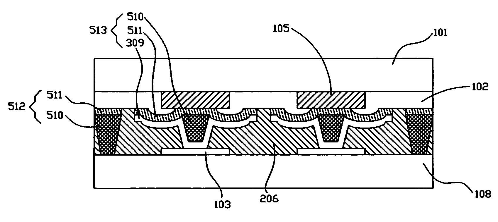
The present invention provides a bonding structure with compliant bumps containing a stopper structure and a protection layer. The compliant bump includes a polymer bump, a metal layer, and a conductive layer. The metal layer is located beneath the polymer bump to serve the purposes of bonding the first substrate and electrical conduction. The conductive layer covers the polymer bump surface to serve the purpose of electrical conduction to the electrode of the second substrate. The covering area ranges from 0.1% to 99% of the entire compliant bump area. The stopper structure can prevent the compliant bump from cracking during the bonding process. The second protection layer is located outside of the metal bonding pads and can protect the first substrate from damage and provide the ground connection. The bonding structure and the first substrate together form a component, which can be bonded using various methods. The compliant bump, the stopper, and the second protection layer can have different shapes and can be used for bonding various substrates. The present invention reduces manufacturing costs and improves the yield rate of bonding.

Problems solved by technology

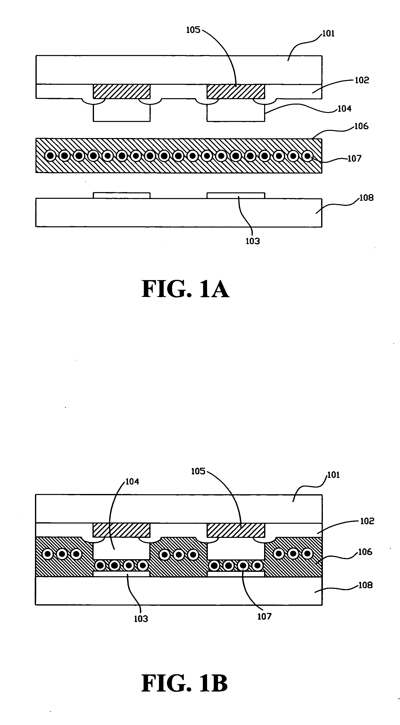
The disadvantage of this technique is that it can not meet finer pitch requirement.
Thus, the technique can not meet finer pitch requirement.
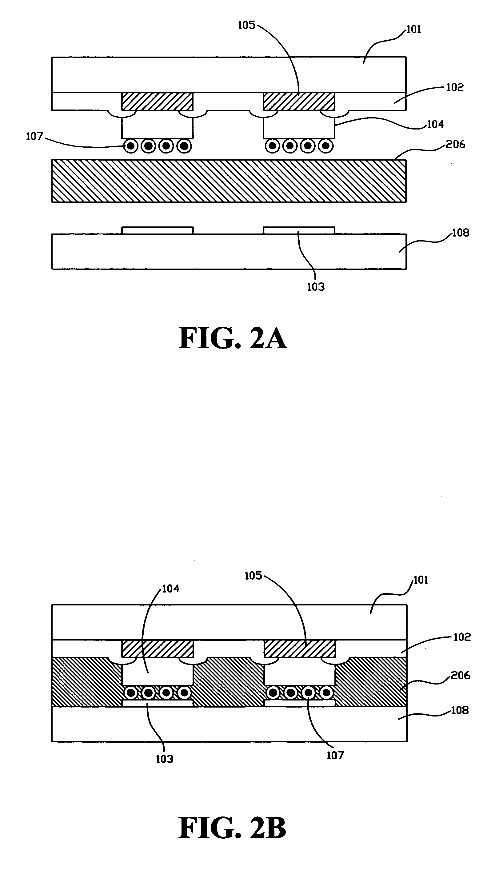
The disadvantage of the NCF bonding technique is that conductive particles 107 will be lost and escape from metal bumps 104 because of the pressure and heat.
Because metal bumps are hard and make it difficult for processing, therefore bumps made of flexible polymer are widely used.
The disadvantage of this technique is that when the bonding pressure is too large, the conductive layer covering the bumps tends to crack, which will lead to increase the resistance or even become non-conductive.

Method used


Image

  • Bonding structure with compliant bumps
  • Bonding structure with compliant bumps
  • Bonding structure with compliant bumps

Examples


first embodiment

[0035]FIG. 11A shows a top view of a rectangular compliant bump 1013. Rectangular compliant bump 1113A has two parallel rows of spheres 1115, and the stoppers are distributed outside of the compliant bump. Conductive layer 309 only covers half of each sphere 1115, and the outer half of spheres 1115 is not covered.

second embodiment

[0036]FIG. 11B shows a top view of a rectangular compliant bump 1013. Rectangular compliant bump 1113B has two parallel rows of spheres 1115, and the stripe stoppers 1112 are distributed on both ends, inside the compliant bump 1113B. Conductive layer 309 covers the entire spheres 1115, but not the stoppers 1112.

third embodiment

[0037]FIG. 11C shows a top view of a rectangular compliant bump 1013. Rectangular compliant bump 1113C has three skewed parallel rows of spheres 1115, and the stripe stoppers 1112 are distributed on both ends, inside the compliant bump 1113C. Conductive layer 309 covers the entire spheres 1115, but not the stoppers 1112. The stripe stoppers 1112 must be arranged in the direction orthogonal to the neighboring side of the first substrate to facilitate the expelling of flowing adhesive material.


PUM


Abstract

The invention provides a bonding structure with compliant bumps, and also includes a stopper structure and a protection layer. Compliant bumps include at least a polymer bump, a metal layer and a surface conductive layer. Both the stopper structure and protection layer are formed with polymer bumps and metal layer. Compliant bumps provide bonding pad and conductive channel. Stoppers are used to prevent compliant bumps from crushing for overpressure in bonding process. The protection layer provides functions of grounding and shielding. The stoppers can be outside or connected with the compliant bumps. The protection layer is lower then the stopper structure and compliant bumps. It can be separated or connected with stoppers.

Description

FIELD OF THE INVENTION [0001] The present invention relates to a bonding structure with compliant bumps for bonding semiconductor material or metal surface to substrate, and the bonding structure includes a stopper structure and a protection layer. It can be applied to bond integrated circuit (IC) or chip to substrate. BACKGROUND OF THE INVENTION [0002] Integrated circuits (IC) are conventionally made of semiconductors wafers. The manufacturing process of IC includes two steps. The first step is to manufacture the semiconductor wafer using semiconductor material, and the second step is using packaging technologies to package. The packaging technologies of the second step are mainly to dice the wafer into chips and then bond the chips to the substrate. The bonding pads are used to bond the chips to the substrate. The bottom layer of the bonding pads are usually made of aluminum covered with passivated metal. For low-profile chips, the bonding pads with a solder bump can bond the chip...

Claims


Application Information

Patent Timeline
Patent Type & Authority Applications(United States)
IPC IPC(8): H01L21/60H01L23/485H01L23/498H05K3/30H05K3/32
CPCH01L23/49816H01L2224/81139H01L24/81H01L24/83H01L2224/131H01L2224/1319H01L2224/1357H01L2224/16225H01L2224/73204H01L2224/81801H01L2224/83101H01L2224/8319H01L2224/838H01L2924/01013H01L2924/01082H01L2924/0781H01L2924/14H01L2924/3025H05K3/305H05K3/325H05K2201/0133H05K2201/0367H05K2201/10674H05K2201/2036H05K2203/1189H01L24/12H01L2224/81136H01L2224/10135H01L2924/10253H01L2224/2919H01L2224/81903H01L2924/014H01L2924/01033H01L2924/00013H01L2224/83851H01L24/29H01L2224/13016H01L2924/00014H01L2224/13099H01L2924/3512H01L2924/00H01L24/05H01L2224/023H01L2224/05022H01L2224/051H01L2224/05572H01L2224/056H01L2224/1411H01L2924/0001
Inventor CHANG, SHYH-MINGHUANG, YUAN-CHANGCHEN, WEN-CHIHYANG, SHENG-SHU
Owner IND TECH RES INST
Learn More