Method for manufacturing semiconductor device

a manufacturing method and semiconductor technology, applied in semiconductor devices, semiconductor/solid-state device details, electrical devices, etc., can solve the problems of large increase in the number of processes required, difficulty in detecting alignment marks, and reducing throughput, cost, yield, etc., to reduce the number of manufacturing processes required and reduce the effect of alignment accuracy

Active Publication Date: 2005-05-12
RENESAS ELECTRONICS CORP
View PDF15 Cites 17 Cited by
  • Summary
  • Abstract
  • Description
  • Claims
  • Application Information

AI Technical Summary

Benefits of technology

[0020] The present invention has been devised in view of the above problems. It is, therefore, an object of the present invention to provide a semiconductor device and a manufacturing method therefor capable of providing a reduced number of manufacturing processes required without reducing the alignment accuracy when the gate electrodes are formed.

Problems solved by technology

However, general-purpose memories such as DRAMs (Dynamic Random Access Memories), SRAM (Static Random Access Memories), and flash memories use polycide or polymetal as their gate electrode material, which makes it difficult to detect the alignment marks since these materials have a high light reflectance level.
As a result, the total number of processes required greatly increases, leading to the problem of a reduction in the throughput, cost, yield, etc.

Method used


Image

  • Method for manufacturing semiconductor device
  • Method for manufacturing semiconductor device
  • Method for manufacturing semiconductor device

Examples


first embodiment

[0127] Description will be made of a method for manufacturing a semiconductor device according to a first embodiment of the present invention with reference to FIGS. 1 to 11. It should be noted that in these figures, like numerals will be used to denote like components.

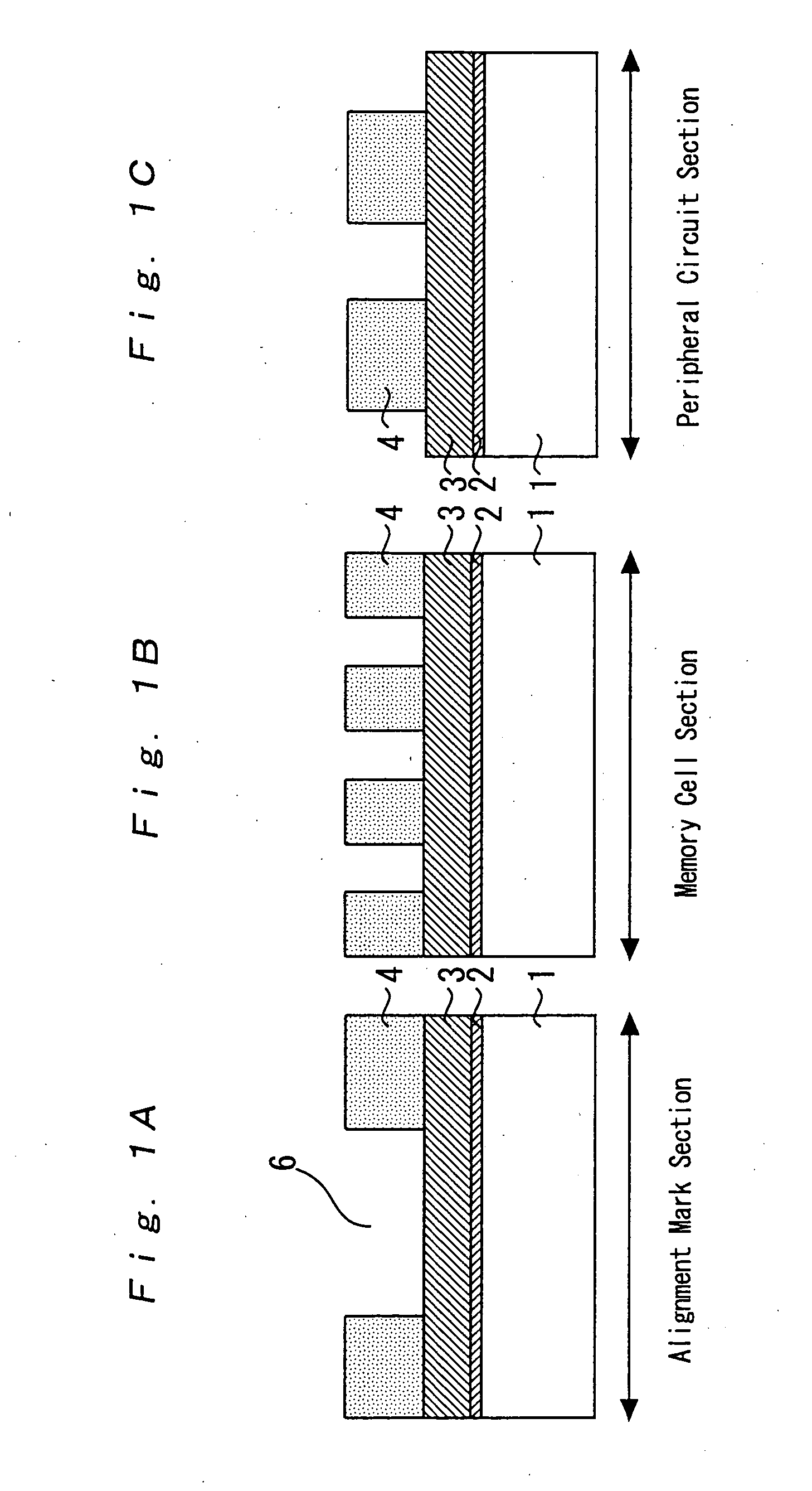
[0128] As shown in FIGS. 1A to 1C, first a silicon oxide film 2 is formed on a semiconductor substrate 1 of a first conductive type as a first insulation film. Then, a silicon nitride film 3 is formed on the silicon oxide film 2. The silicon nitride film 3 is used to form a hard mask.

[0129] A silicon substrate may be used as the semiconductor substrate 1. Further, the silicon oxide film 2 may be formed by the thermal oxidation method such that it has a film thickness of approximately 20 nm. Still further, the silicon nitride film 3 may be formed by the CVD (Chemical Vapor Deposition) method such that it has a film thickness of approximately 100 nm.

[0130] Then, active region patterns are formed on the semiconductor ...

second embodiment

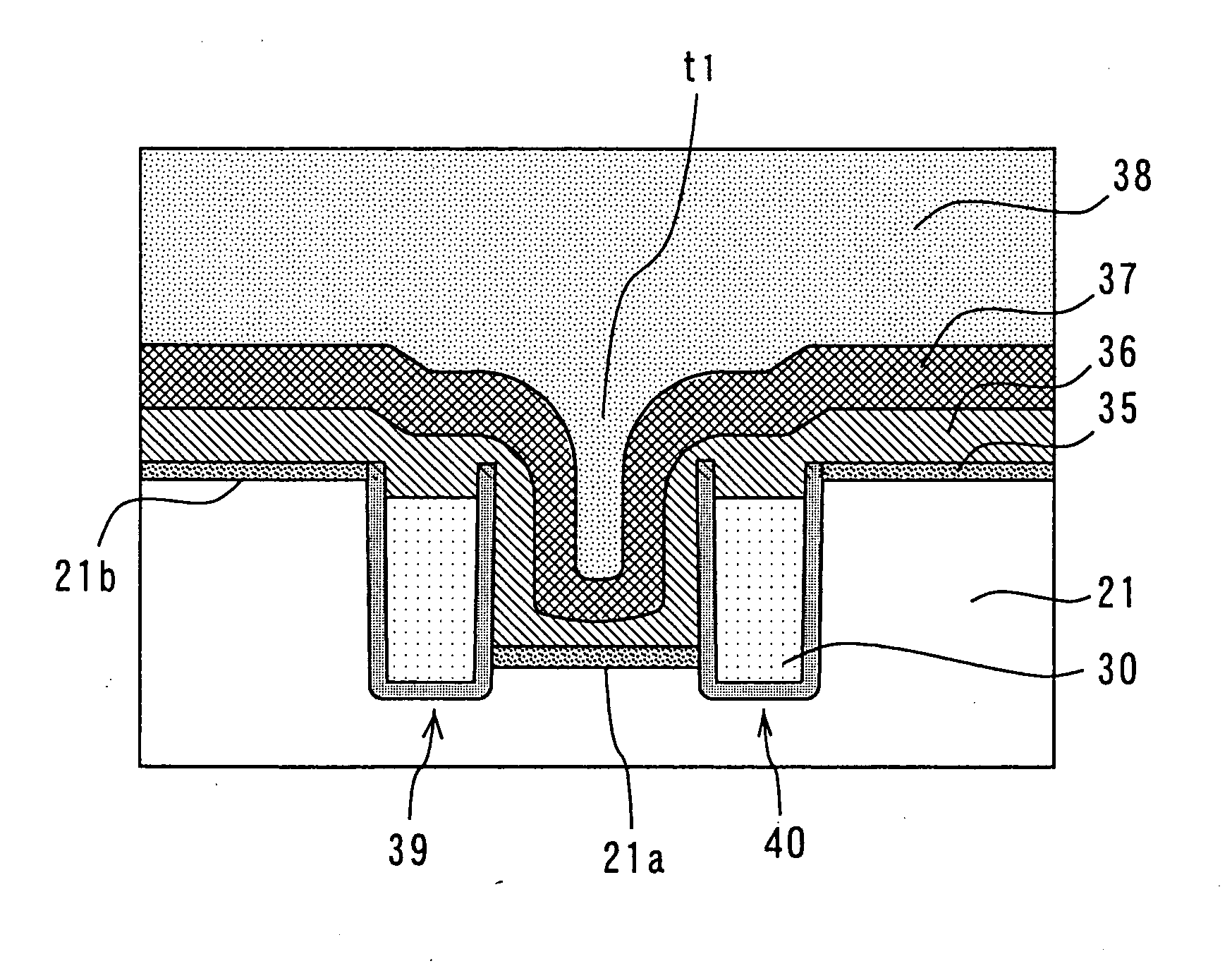
[0153] Description will be made of a method for manufacturing a semiconductor device according to a second embodiment of the present invention with reference to FIGS. 12 to 21. It should be noted that in these figures, like numerals will be used to denote like components.

[0154] First of all, as in the first embodiment, a silicon oxide film 22 is formed on a semiconductor substrate 21 of a first conductive type as a first insulation film. Then, a silicon nitride film 23 is formed on the silicon oxide film 22. The silicon nitride film 23 is used to form a hard mask. A silicon substrate may be used as the semiconductor substrate 21.

[0155] Then, active region patterns are formed on the semiconductor substrate 21 by use of a photolithographic technique. Specifically, first a resist pattern 24 is formed on the silicon nitride film 23, producing the structures shown in FIGS. 12A to 12C. It should be noted that FIGS. 12A, 12B, and 12C show the portions of the resist pattern (24) in the al...

third embodiment

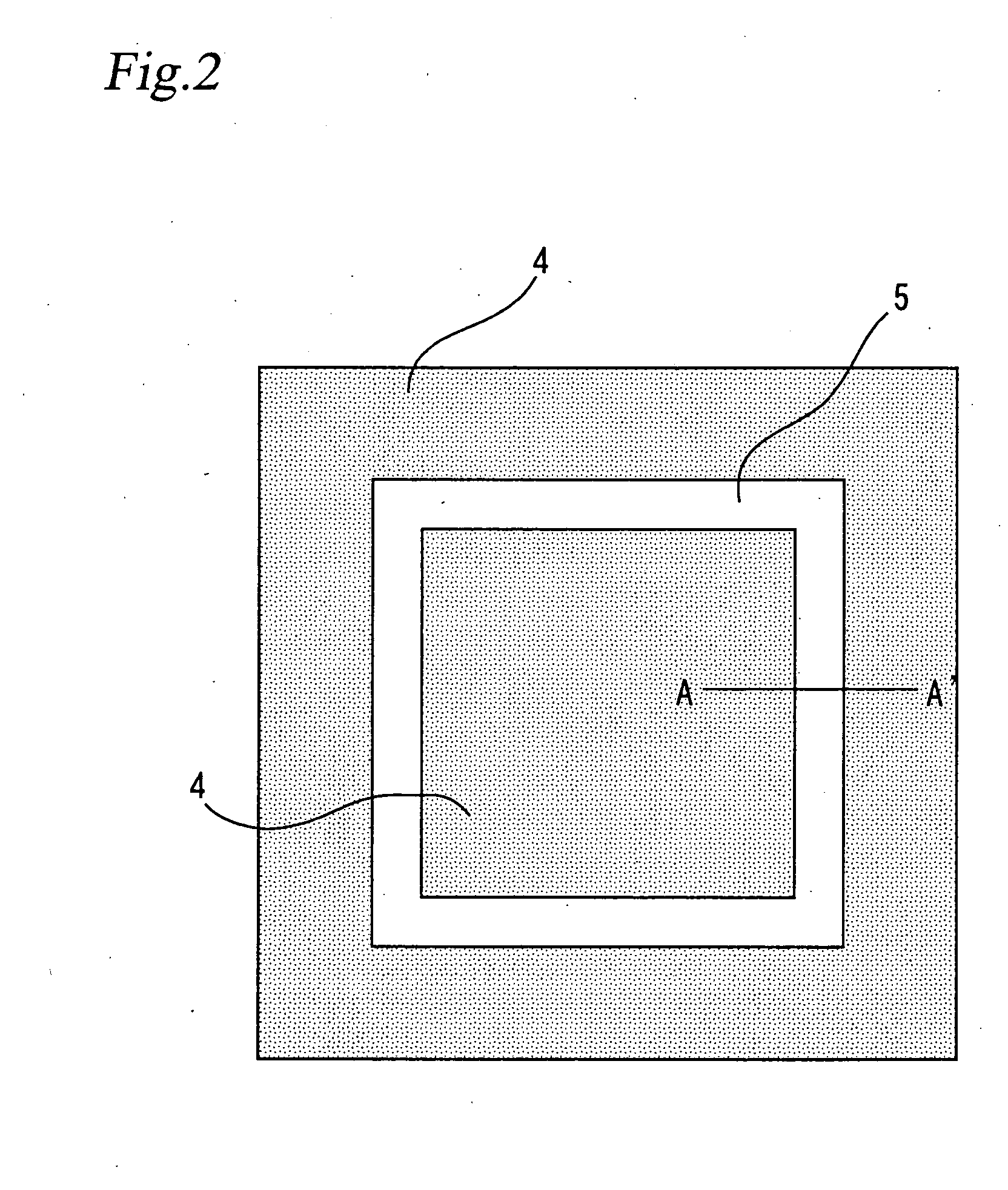
[0173] The alignment mark section of a third embodiment of the present invention employs the same patterns as those shown in FIG. 2 described in connection with the first embodiment.

[0174] Description will be made of a method for manufacturing a semiconductor device according to the present embodiment with reference to FIGS. 22 to 27. It should be noted that in these figures, like numerals will be used to denote like components.

[0175] First of all, a first insulation film and a hard mask are sequentially formed on a semiconductor substrate of a first conductive type. Then, the first insulation film and the semiconductor substrate are etched using the hard mask, forming grooves having a predetermined depth in the alignment mark section and the device formation section of the semiconductor substrate. After burying a second insulation film into the grooves, the hard mask is removed. For example, as shown in FIGS. 22A to 22C, active region patterns are formed on a semiconductor substr...


PUM


Abstract

An alignment mark section on a semiconductor substrate has two grooves which are filled with silicon oxide. The surface of the portion of the semiconductor substrate sandwiched by these grooves is lower than other portions of the semiconductor substrate to produce a step having a predetermined depth in the alignment mark section.

Description

BACKGROUND OF THE INVENTION [0001] 1. Field of the Invention [0002] The present invention relates to a method for manufacturing a semiconductor device, and more particularly to a method for manufacturing a semiconductor device having a device formation section (or region) and an alignment mark section on its semiconductor substrate. [0003] 2. Background Art [0004] In recent years, semiconductor devices have become smaller and smaller as their integration density has increased and each semiconductor region of the devices has been miniaturized. The transistor characteristics of a miniaturized semiconductor device is significantly affected by the alignment between the active regions and the gate electrodes, as described in detail below. [0005] Each gate electrode (of a semiconductor device) is formed on a predetermined area of an active region. Therefore, when the gate electrode material is patterned, it is necessary to carry out the process of aligning the gate electrode material with...

Claims


Application Information

Patent Timeline
Patent Type & Authority Applications(United States)
IPC IPC(8): H01L21/00H01L21/301H01L21/46H01L21/76H01L21/027H01L21/78H01L21/8242H01L23/544H01L27/10H01L27/108
CPCH01L23/544H01L2223/54453Y10S438/975H01L2924/0002H01L2924/00H01L2223/54426
Inventor OHTO, KENICHITERAUCHI, TAKASHI
Owner RENESAS ELECTRONICS CORP
Why Eureka
Try Eureka