Orientation dependent shielding for use with dipole illumination techniques

a dipole illumination and orientation-dependent shielding technology, applied in the field of photolithography, can solve the problems of reducing the size of an integrated circuit, cd (critical dimension) of the corresponding mask pattern approaching the resolution limit of the optical exposure tool, and single illumination only enhancing resolution

Inactive Publication Date: 2005-05-12
ASML NETHERLANDS BV
View PDF10 Cites 57 Cited by
  • Summary
  • Abstract
  • Description
  • Claims
  • Application Information

AI Technical Summary

Benefits of technology

[0023] In an effort to solve the foregoing needs, it is one object of the present invention to provide a shielding technique that does not result in an increase in the number of exposures or masks required for imaging the wafer, and that does not impact the use and / or placement of assist features with the mask design.
[0024] More specifically, in one exemplary embodiment, the present invention relates to a method of printing a pattern having vertically oriented features and horizontally oriented features on a substrate utilizing dipole illumination, which includes the steps of: identifying background areas contained in the pattern; generating a vertical component mask comprising non-resolvable horizontally oriented features in the background areas; generating a horizontal component mask comprising non-resolvable vertically oriented features in the background areas; illuminating said vertical component mask utilizing an X-pole illumination; and illuminating said horizontal component mask utilizing a Y-pole illumination. As explained in detail below, the non-resolvable features added to the background portion of the mask patterns function to reduce the background light incident on the wafer and negate the effects of lens flare.
[0030] The method of the present invention provides important advantages over the prior art. For example, the present invention provides a simple method for reducing the negative effects associated with lens flare without increasing the number of masks necessary to print the desired pattern. In addition, the method of the present invention provides background shielding in such a manner that it does not effect the placement or use of assist features with the mask.
[0031] Furthermore, the flare reduction method of the present invention is easily integrated into the current design flow, does not result in reticle manufacturability issues, and has minimum data volume impact.
[0032] The present invention further provides a methodology to reduce the impact of flare and produce better process latitude and provide CD control and improve device performance.

Problems solved by technology

These rules are set by processing and design limitations.
As the size of an integrated circuit is reduced and its density increases, however, the CD (critical dimension) of its corresponding mask pattern approaches the resolution limit of the optical exposure tool.
However, one of the limitations associated with dipole illumination is that a single illumination only enhances resolution for features that are orthogonal to the illumination pole axis.
As a result of the need to separate the horizontally and vertically oriented features, one of the challenges for the lithographer, when utilizing dipole illumination, is determining how to convert the original IC design data into its horizontal or vertical pattern components and generate two masks for the dual exposure process that can take full advantage of the dipole imaging performance.
One factor that reduces performance and which should be considered when generating the mask patterns is background light due to lens flare or scattering.
As: is known, lens flare results in unwanted background light (i.e., noise) that degrades the image contrast at the image plane.
The overall effect is an unwanted DC background light that reduces the aerial image contrast.
Furthermore, besides the negative impact on image contrast, flare is also unevenly distributed across the scanning slit and is not uniform with the exposure field, which can cause intrafield CD variations.
Therefore, protecting features and reducing background stray light becomes increasingly critical.
Thus, such a solution for reducing the effects of flare is undesirable as it results in an increase in the number of exposures and masks required for imaging the wafer.
Furthermore, the foregoing solid chrome shielding technique can also negatively interfere with assist features, such as scatter bars, and cause the assist features to print underneath the shielding of either the horizontal or vertical mask, as-also illustrated in FIGS. 3a and 3b.
This problem imposes an additional constraint on the placement of assist features, which can prevent the assist features from being placed in the optimal position, thereby causing a reduction in printing performance.

Method used


Image

  • Orientation dependent shielding for use with dipole illumination techniques
  • Orientation dependent shielding for use with dipole illumination techniques
  • Orientation dependent shielding for use with dipole illumination techniques

Examples


Embodiment Construction

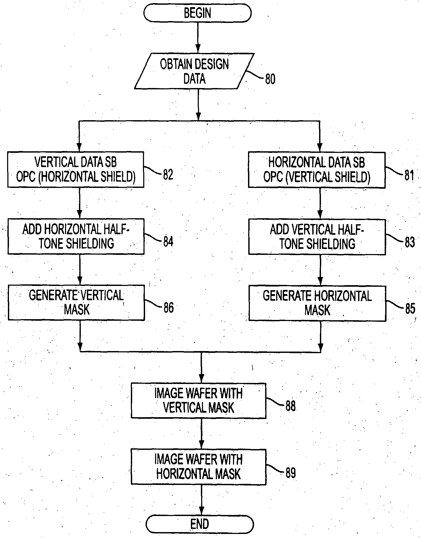
[0053] In accordance with the present invention, the negative effects of lens flare are significantly reduced by utilizing a sub-resolution grating block (SGB) in the background areas of the mask design. As explained in more detail below, the SGB comprises a plurality of non-resolvable shielding lines disposed in the background portion of the mask, which have an orientation orthogonal to the features being imaged by the given mask. The non-resolvable shielding lines do not print on the wafer, but do provide the necessary shielding effect required to eliminate the effects of flare.

[0054] Prior to a description of exactly how the SGB is applied to a given mask, a brief explanation regarding the theory behind the present invention is provided. In order to reduce the background light level, it is necessary to control the amount of the zero order (i.e., DC level) light transmitted by the reticle. Long-range flare does not vary over lateral-distances comparable to the wavelength (>0.5 mm...


PUM

PropertyMeasurementUnit
wavelengthaaaaaaaaaa
widthaaaaaaaaaa

Abstract

A method of printing a pattern having vertically oriented features and horizontally oriented features on a substrate utilizing dipole illumination, which includes the steps of: identifying background areas contained in the pattern; generating a vertical component mask comprising non-resolvable horizontally oriented features in the background areas; generating a horizontal component mask comprising non-resolvable vertically oriented features in the background areas; illuminating said vertical component mask utilizing an X-pole illumination; and illuminating said horizontal component mask utilizing a Y-pole illumination.

Description

FIELD OF THE INVENTION [0001] The present invention relates to photolithography, and in particular relates to the generation of mask layouts, for use with dipole illumination techniques, that provide for a reduction in the loss of image contrast caused by lens flare, which can be significant when utilizing dipole illumination due to the multiple exposures. In addition, the present invention relates to a device manufacturing method using a lithographic apparatus comprising a radiation system for providing a projection beam of radiation; a mask table for holding a mask, serving to pattern the projection beam; a substrate table for holding a substrate; and a projection system for projecting the patterned projection beam onto a target portion of the substrate. BACKGROUND OF THE INVENTION [0002] Lithographic projection apparatus (tools) can be used, for example, in the manufacture of integrated circuits (ICs). In such a case, the mask contains a circuit pattern corresponding to an indivi...

Claims


Application Information

Patent Timeline
Patent Type & Authority Applications(United States)
IPC IPC(8): G03F1/00G03F1/36G03F7/20H01L21/027
CPCG03F1/144G03F1/36G03F7/70941G03F7/70425G03F7/70466G03F7/70125G03F1/70G03F1/68G03F1/00G03F1/32
Inventor HSU, STEPHEN DUAN-FUCORCORAN, NOELCHEN, JANG FUNG
Owner ASML NETHERLANDS BV
Why Eureka
Try Eureka