Integrated circuit carrier apparatus method and system

a technology of integrated circuits and apparatuses, applied in the field of electronic circuits and systems, can solve the problems of inability to achieve a corresponding increase in density on board level products, many of the improvements in packaging technology have proved too expensive to be useful for commodity parts and circuits, and the physical contact has become increasingly impractical, so as to facilitate analysis and testing of integrated circuits, and facilitate design of low-cost integrated circuit carriers

Active Publication Date: 2005-05-19
BELL SEMICON LLC
View PDF8 Cites 9 Cited by
  • Summary
  • Abstract
  • Description
  • Claims
  • Application Information

AI Technical Summary

Benefits of technology

[0019] Furthermore, the method for designing an integrated circuit carrier with backside access to an integrated circuit may also include routing traces between a ring of die connection pads and an array of package connection pads without penetrating the access region. The various method steps facilitate designing low-cost integrated circuit carriers and packages using readily available manufacturing and testing processes.
[0020] In another aspect of the invention, a method for packaging and providing backside access t...

Problems solved by technology

Despite the tremendous increase in device density achievable with semiconductors, integrated circuit packaging has limited the ability to achieve a corresponding increase in density on board level products.
However, many of these improvements in packaging technology have proven to be too expensive to be useful for commodity parts and circuits.
Such physical contact has become increasingly impractical and may damage the devices or signal paths under test.
However, despite the tremendous advantage available with laser interfereometry, backside access to an integrated circuit die is required ...

Method used


Image

  • Integrated circuit carrier apparatus method and system
  • Integrated circuit carrier apparatus method and system
  • Integrated circuit carrier apparatus method and system

Examples


Embodiment Construction

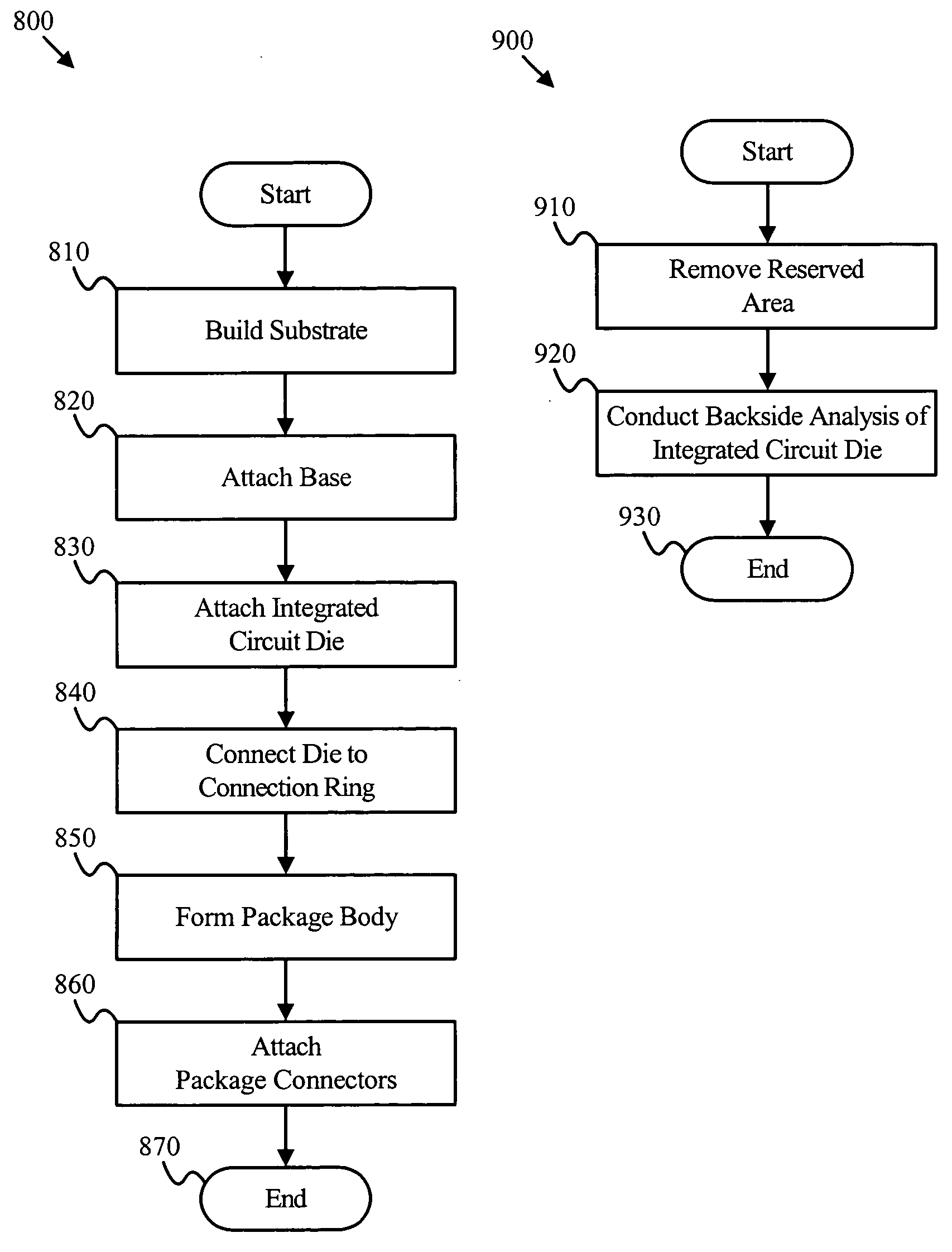
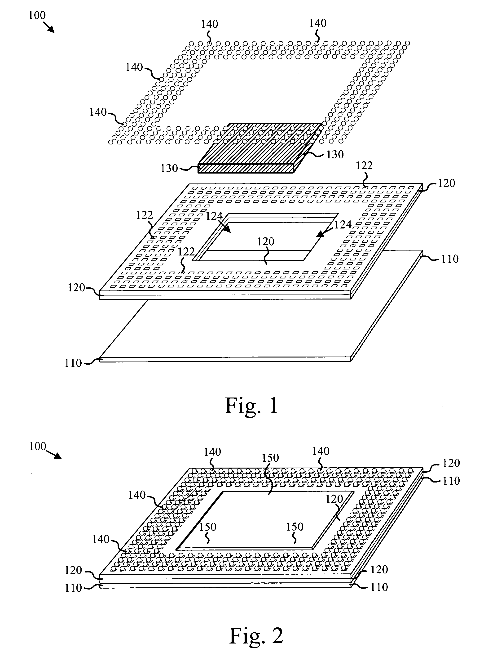
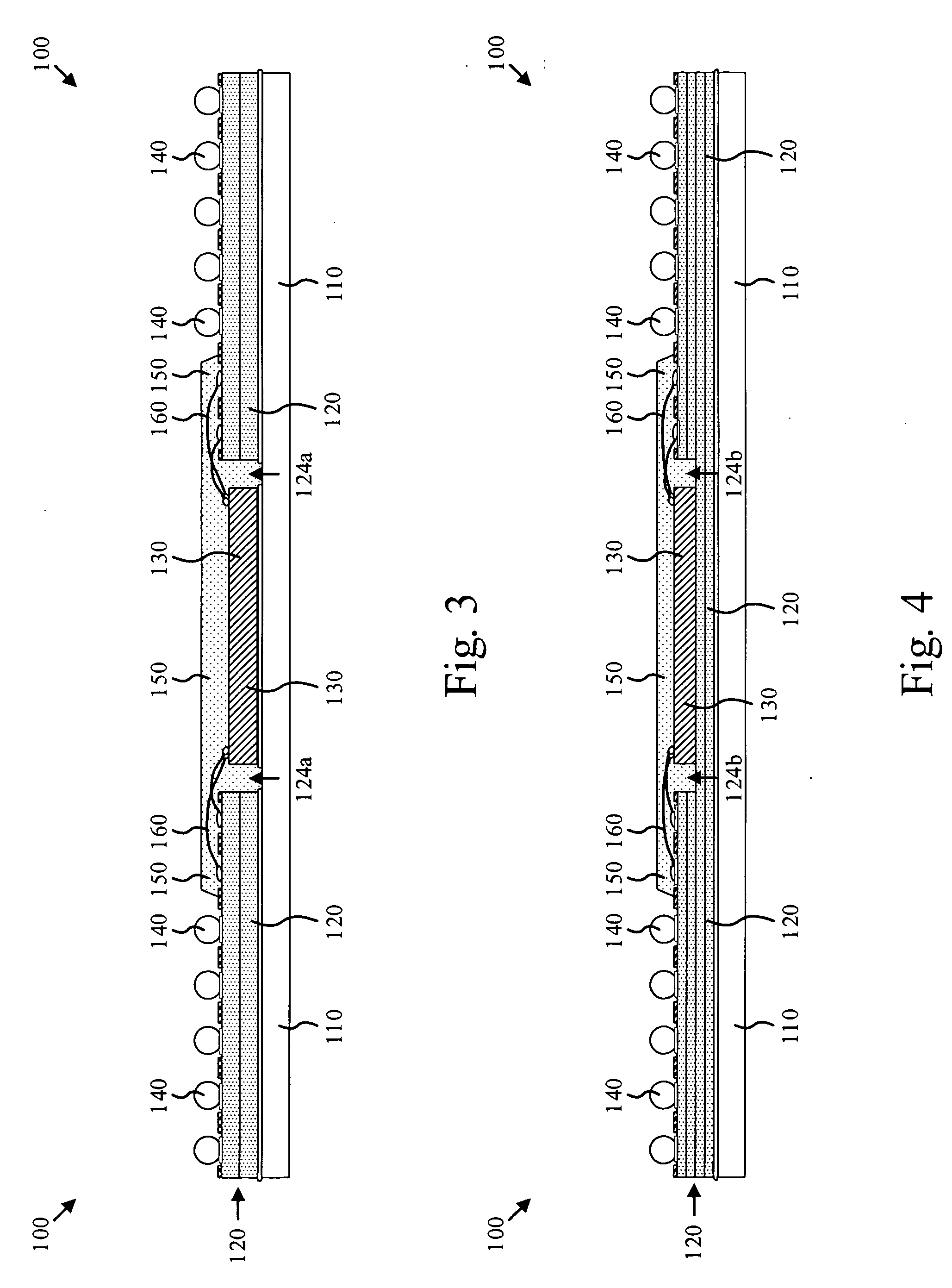
[0035] It will be readily understood that the components of the present invention, as generally described and illustrated in the Figures herein, may be arranged and designed in a wide variety of different configurations. Thus, the following more detailed description of the embodiments of the apparatus, method, and system of the present invention, as represented in FIGS. 1 through 11, is not intended to limit the scope of the invention, as claimed, but is merely representative of selected embodiments of the invention.

[0036] Reference throughout this specification to “one embodiment” or “an embodiment” means that a particular feature, structure, or characteristic described in connection with the embodiment is included in at least one embodiment of the present invention. Thus, appearances of the phrases “in one embodiment” or “in an embodiment” in various places throughout this specification are not necessarily all referring to the same embodiment and the described features, structure...


PUM


Abstract

A carrier substrate includes an access region placed within the interior of the substrate that facilitates backside access to an integrated circuit die without damaging electrical integrity of the carrier substrate, a ring of die connection pads placed around the access region, and an array of package connection pads positioned around the perimeter of the top surface of the carrier substrate. In one embodiment, the perimeter depth of the array of package connections pads is selected to correspond to the number of electrical traces routable between minimally spaced package connection pads. The basic carrier substrate design is used to create an integrated circuit carrier family with each particular circuit carrier configured to receive a range of integrated circuit sizes and I/O counts such that each circuit carrier overlaps in size range with at least one other circuit carrier.

Description

BACKGROUND OF THE INVENTION [0001] 1. Field of the Invention [0002] The present invention relates generally to electronic circuits and systems. Specifically, the invention relates to apparatus, methods, and systems for packaging and testing integrated circuits. [0003] 2. Description of the Related Art [0004] Semiconductor circuit technologies have experienced a steady march of process and materials improvements since their introduction in the later half of the 20th century. Such improvements have significantly decreased the geometry sizes of semiconductor devices while dramatically increasing the density, clock rates, and processing power attainable on a single chip. Despite the tremendous increase in device density achievable with semiconductors, integrated circuit packaging has limited the ability to achieve a corresponding increase in density on board level products. [0005] To address the needs resulting from improvements in semiconductor technology, a number of changes in packag...

Claims


Application Information

Patent Timeline
IPC IPC(8): H01L23/31H01L23/36H01L23/498
CPCH01L23/3128H01L2224/05554H01L23/49816H01L23/49838H01L24/06H01L24/49H01L2224/0401H01L2224/04042H01L2224/32225H01L2224/48091H01L2224/48227H01L2224/49171H01L2224/49431H01L2224/49433H01L2224/73265H01L2924/01029H01L2924/014H01L2924/14H01L2924/1433H01L2924/15153H01L2924/1517H01L2924/15173H01L2924/15311H01L2924/1532H01L2924/3011H01L2924/3025H01L23/36H01L2924/01033H01L24/48H01L2924/00014H01L2924/00H01L2924/10162H01L2924/12042H01L2924/181H01L2224/45099H01L2224/05599H01L2924/00012
Inventor AWUJOOLA, ABIOLAFISHLEY, CLIFFORD R.
Owner BELL SEMICON LLC
Why Eureka
Try Eureka