Methods for patterning substrates having arbitrary and unexpected dimensional changes

a technology of dimensional change and patterning, applied in the field of system for fabricating electronic modules on substrates, can solve the problems of not providing any means for fine adjustment of magnification, unable to address local or global problems, and deviation from 1, etc., and achieves low cost, low cost, and large area

Inactive Publication Date: 2005-05-19
SONY CORP +1
View PDF24 Cites 80 Cited by
  • Summary
  • Abstract
  • Description
  • Claims
  • Application Information

AI Technical Summary

Benefits of technology

[0011] Embodiments of the present invention provide a method for creating electronic modules, such as displays and semiconductor devices, that can be fabricated at low cost on a variety of substrates including flexible printable circuit (FPC) plastics, metals, ceramics, paper, and glass. In one embodiment, the system can be used in the manufacture of high density flex circuits. As a result, it is possible to produce modules of large area at low cost. Fabrication of such modules is enabled by improved lithography systems and methods. The improved lithography system uses a programmable mask mechanism, such as a digital micro-mirror device (DMD) array. As a result, the mask pattern can be modified almost instantaneously, in real time, to account for physical variations or deviations of a mask pattern on the substrate relative to its expected or ideal pattern.
[0012] A method for patterning a plurality of electronic elements on a substrate is disclosed in accordance with one embodiment of the present invention. As discussed below, the method uses an alignment mechanism containing an optical measurement system and an electronic programmable digital mask system. The method also utilizes an optical measurement device for optically measuring an existing geometric pattern, corresponding to an exposed mask pattern, on a substrate. The existing pattern is written on an nth layer of the substrate. A computing device, coupled to the optical measurement device, calculates a correction between the existing geometric pattern of the substrate and an expected pattern for the nth layer. An image transformation component, coupled to the computing device, performs an image transformation on a mask pattern intended for an (n+1)th layer, based on the calculated correction, to generate a corrected pattern. A writing component, coupled to the image transformation component, writes the corrected pattern onto the (n+1)th layer using a programmable digital mask system. The writing component contains a radiation source. An optical system is coupled to the writing component for guiding radiation from the radiation source to the programmable digital mask and from the programmable digital mask to the substrate. In this way, the corrected pattern for the (n+1)th layer can be written onto the substrate with high alignment accuracy to the nth layer mask.

Problems solved by technology

It does not provide any means for fine adjustment in magnification (deviation from 1:1 magnification) to compensate for slight changes in substrate dimensions.
However, it cannot make local changes from field to field.
This system is primarily concerned with deformation of the substrate perpendicular to the plane of the substrate and, therefore, does not address the problem of local or global expansion / contraction of the substrate primarily within the plane.

Method used


Image

  • Methods for patterning substrates having arbitrary and unexpected dimensional changes
  • Methods for patterning substrates having arbitrary and unexpected dimensional changes
  • Methods for patterning substrates having arbitrary and unexpected dimensional changes

Examples


Embodiment Construction

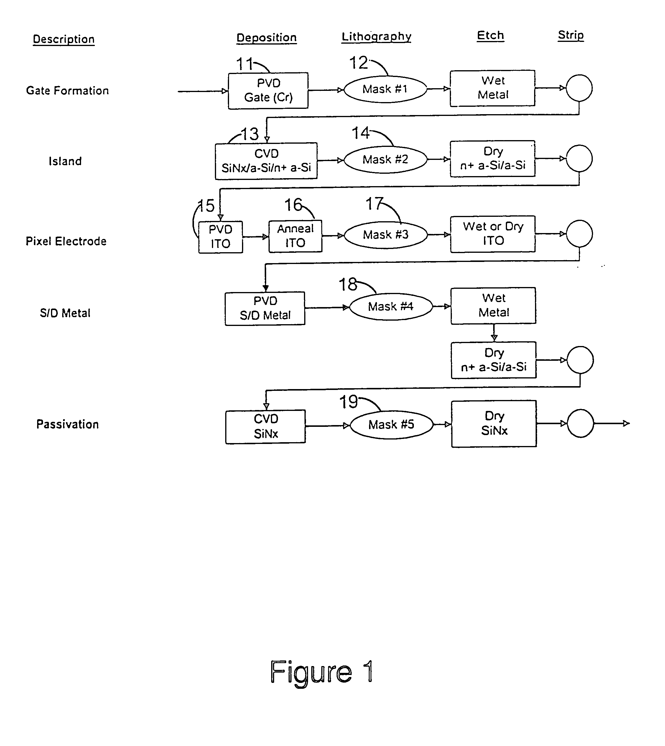
[0027] Reference will now be made in detail to the preferred embodiments of the invention, examples of which are illustrated in the accompanying drawings. While the invention will be described in conjunction with the preferred embodiments, it will be understood that they are not intended to limit the invention to these embodiments. On the contrary, the invention is intended to cover alternatives, modifications and equivalents, which may be included within the spirit and scope of the invention as defined by the appended claims. Furthermore, in the following detailed description of the present invention, numerous specific details are set forth in order to provide a thorough understanding of the present invention. However, it will be obvious to one of ordinary skill in the art that the present invention may be practiced without these specific details. In other instances, well-known methods, procedures, components, and circuits have not been described in detail so as not to unnecessaril...


PUM


Abstract

Methods for patterning a plurality of electronic elements on a deformable substrate. The method uses an optical measurement device for optically measuring an existing geometric pattern on a substrate. The existing pattern is written on an nth layer of the substrate. A computing device, coupled to the optical measurement device, calculates a correction between the existing geometric pattern and an expected pattern for the nth layer. An image transformation component, coupled to the computing device, performs an image transformation on an electronic pattern to be used in an (n+1)th layer, based on the calculated correction, to generate a corrected electronic pattern. A writing component, coupled to the image transformation component, writes the corrected electronic pattern onto the (n+1)th layer using a programmable digital mask system. The writing component contains a radiation source which is coupled to an optical system for guiding radiation from the radiation source to the programmable digital mask and from there to the substrate.

Description

RELATED U.S. APPLICATION [0001] This Application claims priority to the copending provisional patent application Ser. No. 60 / 475,801, Attorney Docket Number SONY-50T5470.PRO, entitled “Exposure Systems and Methods Suitable for Patterning Substrates with Arbitrary and Unexpected Dimensional Changes,” with filing date Jun. 3, 2003, assigned to the assignee of the present application, and hereby incorporated by reference in its entirety. [0002] This Application is related to U.S. Patent Application by Fusao Ishii entitled “System for Fabricating Electronic Modules on Substrates Having Arbitrary and Unexpected Dimensional Changes” with attorney docket no. SONY-50T5469, Ser. No. ______, filed concurrently herewith, and assigned to the assignee of the present invention, hereby incorporated by reference in its entirety.FIELD OF THE INVENTION [0003] An embodiment of the present invention relates to a system for fabricating electronic modules on substrates that have arbitrary and unexpected ...

Claims


Application Information

Patent Timeline
Patent Type & Authority Applications(United States)
IPC IPC(8): G03B27/42G03B27/58G03B27/62G03F7/20G03F9/00G06F9/45G06F17/50
CPCG03F7/2057G03F7/70291G03F7/70783G03F7/70633G03F7/70433
Inventor ISHII, FUSAO
Owner SONY CORP
Why Eureka
Try Eureka