
Optical system for providing a hexapole illumination and method of forming a photoresist pattern on a substrate using the same

Active Publication Date: 2005-05-19
SAMSUNG ELECTRONICS CO LTD
View PDF2 Cites 5 Cited by
  • Summary
  • Abstract
  • Description
  • Claims
  • Application Information

AI Technical Summary

Benefits of technology

[0019] An optical system includes a hexapole illumination apparatus capable of substantially securing a process margin in a photolithography process for forming a photoresist pattern to be used in subsequent processes for forming structures such as contact pads on a substrate.
[0020] A method according to an embodiment of the present disclosure forms a photoresist pattern on a substrate using a hexapole illumination to substantially secure a process margin in a photolithography process.
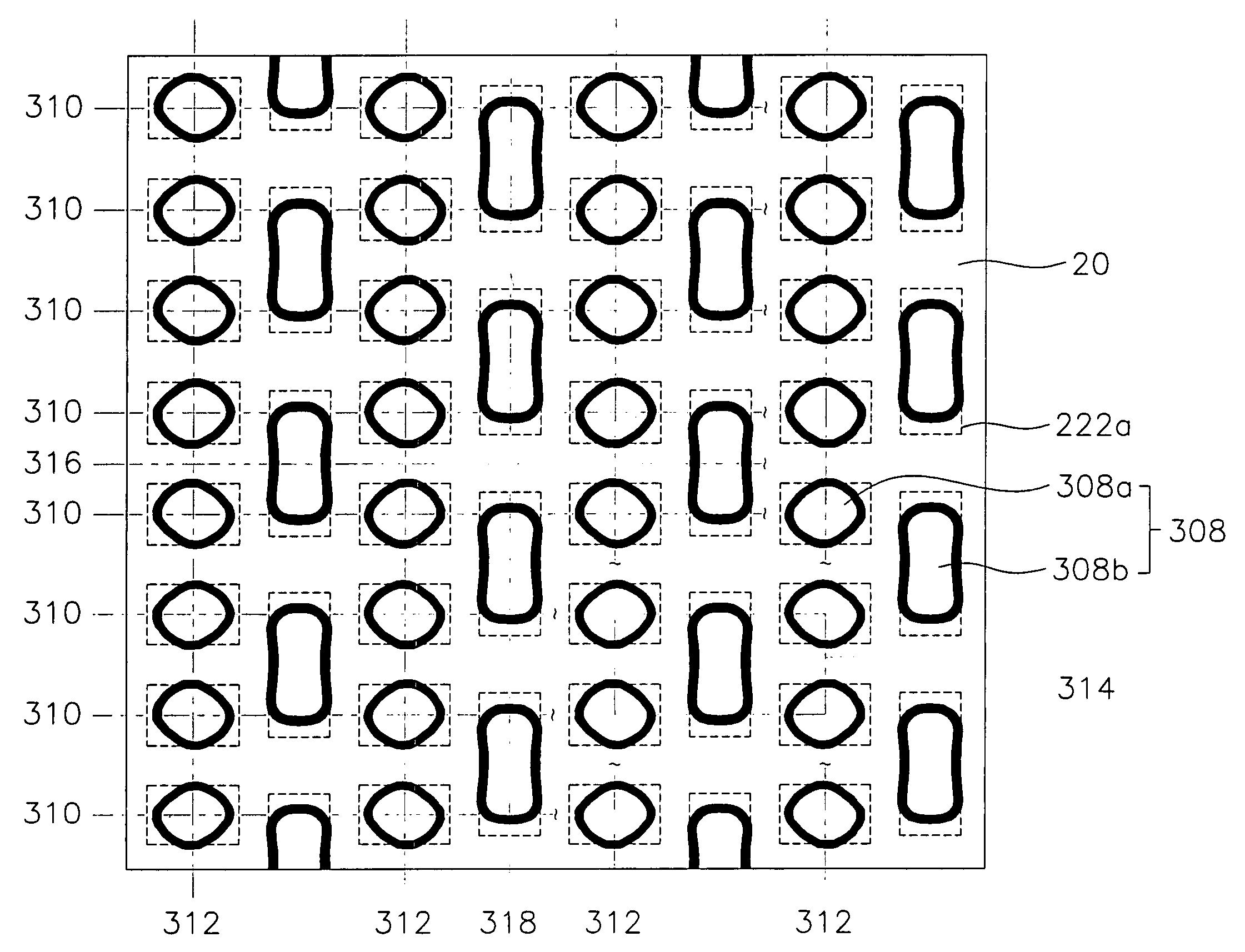
[0029] A resolution of the photoresist pattern including the first holes and the second holes and a depth of focus of the second light beam may be improved by means of the off-axis illumination beam having the hexapole as above-mentioned.

Problems solved by technology

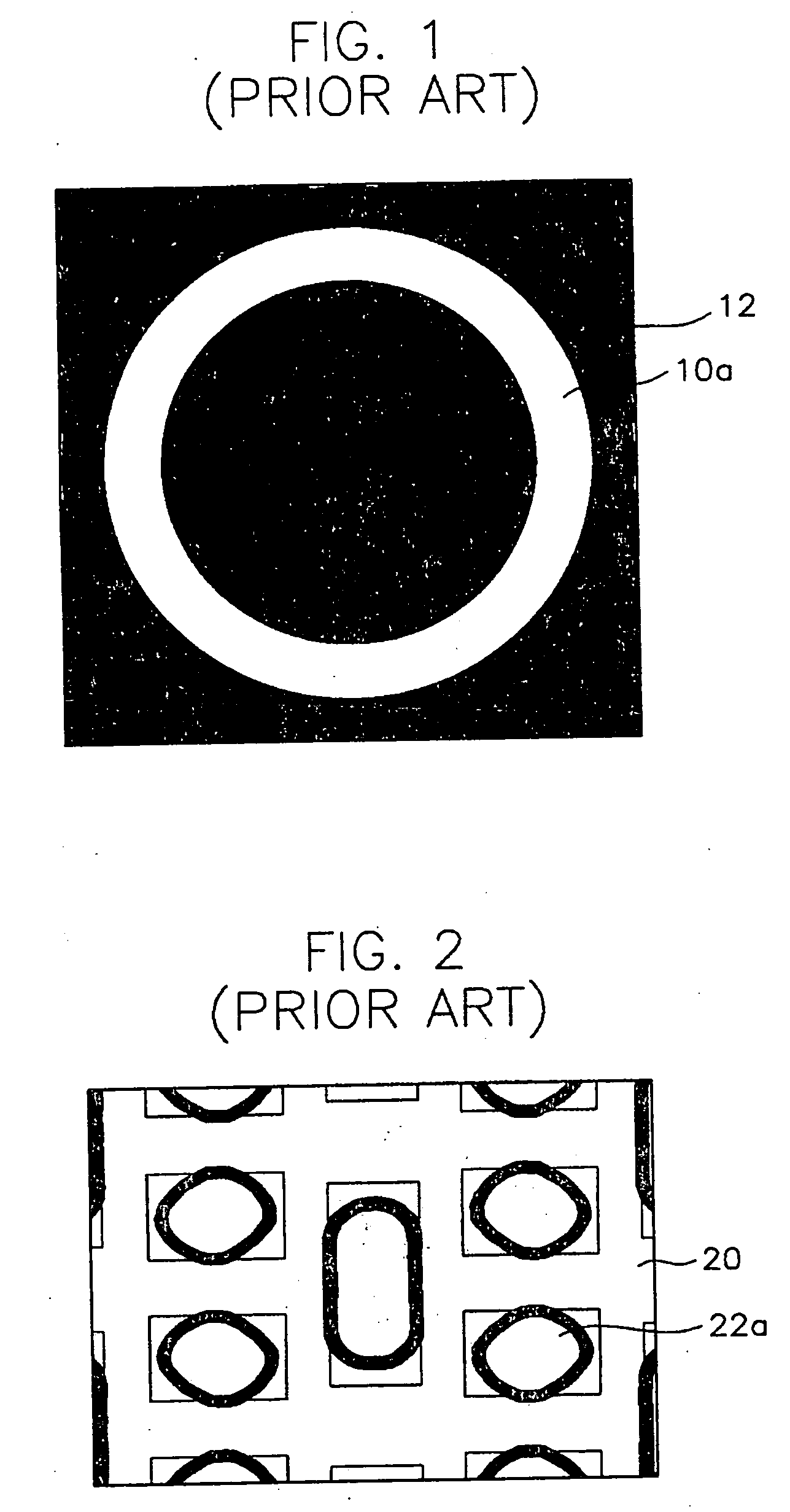
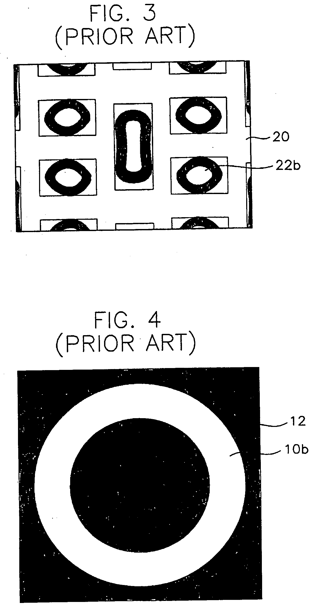
Where a numerical aperture of the projection lens is increased to improve the resolution the DOF may deteriorate.
Thus, the OAI may not cope effectively with complex and / or fine photoresist patterns, and a process margin in the photolithography process may not be sufficiently secured.

Method used


Image

  • Optical system for providing a hexapole illumination and method of forming a photoresist pattern on a substrate using the same
  • Optical system for providing a hexapole illumination and method of forming a photoresist pattern on a substrate using the same
  • Optical system for providing a hexapole illumination and method of forming a photoresist pattern on a substrate using the same

Examples


Embodiment Construction

[0052] The present invention now will be described more fully hereinafter with reference to the accompanying drawings in which preferred embodiments of the disclosure are shown. This invention may, however, be embodied in many different forms and should not be construed as limited to the embodiments set forth herein; rather, these embodiments are provided so that this disclosure will be thorough and complete, and will fully convey the scope of the invention to those skilled in the art.

[0053]FIG. 7 is a schematic view of an optical system according to an embodiment of the present disclosure, FIG. 8 is a cross-sectional view of an off-axis illumination beam having a hexapole, and FIG. 9 is a plan view showing a photoresist pattern formed using the off-axis illumination beam as shown in FIG. 8.

[0054] Referring to FIGS. 7 to 9, an exposure apparatus 200 for forming a photoresist pattern on a semiconductor substrate 20 includes an optical system 210 for irradiating a light beam onto a ...


PUM


Abstract

In an optical system for forming a photoresist pattern on a substrate, an optical element such as a holographic optical element and an aperture plate provides an off-axis illumination beam having a hexapole. The photoresist pattern is formed to form structures such as contact pads, and includes first holes and second holes repeatedly arranged on the substrate. The hexapole includes four first poles symmetrically disposed with respect to an x-axis and a y-axis, and two second poles disposed in the x-axis so as to be symmetric with respect to the y-axis. The off-axis illumination beam may improve a resolution of the photoresist pattern and a depth of focus (DOF) of a light beam to be projected onto the substrate.

Description

BACKGROUND OF THE INVENTION [0001] 1. Field of the Invention [0002] The present invention relates to an exposure apparatus for forming a photoresist pattern on a semiconductor substrate. More particularly, the present invention relates to an optical system of an exposure apparatus for forming a photoresist pattern on a silicon wafer used as a semiconductor substrate. [0003] 2. Description of the Related Art [0004] Semiconductor devices may be manufactured by a process including a fabrication process performed for forming electronic circuits on a silicon wafer used as a semiconductor substrate, an electrical die sorting (EDS) process performed for inspecting electrical characteristics of the semiconductor devices on the semiconductor substrate, and a packaging process performed for packaging the semiconductor devices in epoxy resins and individuating the semiconductor devices. [0005] The fabrication process may include various unit processes such as a deposition process, a chemical m...

Claims


Application Information

Patent Timeline
IPC IPC(8): G03B27/42G03C5/00G03F7/20G03F9/00
CPCG03F7/70108G03B27/42
Inventor NAM, DONG-SEOKHWANG, CHANKANG, YOUNG-SEOG
Owner SAMSUNG ELECTRONICS CO LTD
Learn More