Charge dissipative dielectric for cryogenic devices

a dielectric and charge dissipation technology, applied in the direction of superconductor devices, superconductive devices, conductors, etc., can solve the problems of electrostatic charge accumulation, damage or destruction of circuits, and formation of very large potential differences between thin-film layers of devices, so as to reduce the risk of electrostatic discharge

Inactive Publication Date: 2005-05-19
STAR CRYOELECTRONICS
View PDF7 Cites 23 Cited by
  • Summary
  • Abstract
  • Description
  • Claims
  • Application Information

AI Technical Summary

Benefits of technology

[0009] The superconducting metal wiring layers used to fabricate the SQUID circuits are separated by a conductive doped semiconductor film that prevents charge accumulation at room temperature, thereby greatly reducing the risk of electrostatic discharge that may damage the SQUID circuits during normal handling at room temperature. When the SQUID is cooled to its normal operating temperature, the semiconductor film undergoes a metal...

Problems solved by technology

If the dielectric used to electrically isolate the wiring layers of a thin film circuit is a perfect insulator, normal handling of the chips cut from fabricated wafers can lead to the accumulation of electrostatic charg...

Method used


Image

  • Charge dissipative dielectric for cryogenic devices
  • Charge dissipative dielectric for cryogenic devices
  • Charge dissipative dielectric for cryogenic devices

Examples


Embodiment Construction

[0019] Throughout the following description, specific process details are set forth in order to provide a more thorough understanding of the invention. However, the invention may be practiced without these particulars. Accordingly, the specifications and drawings are to be regarded in an illustrative, rather than a restrictive, sense.

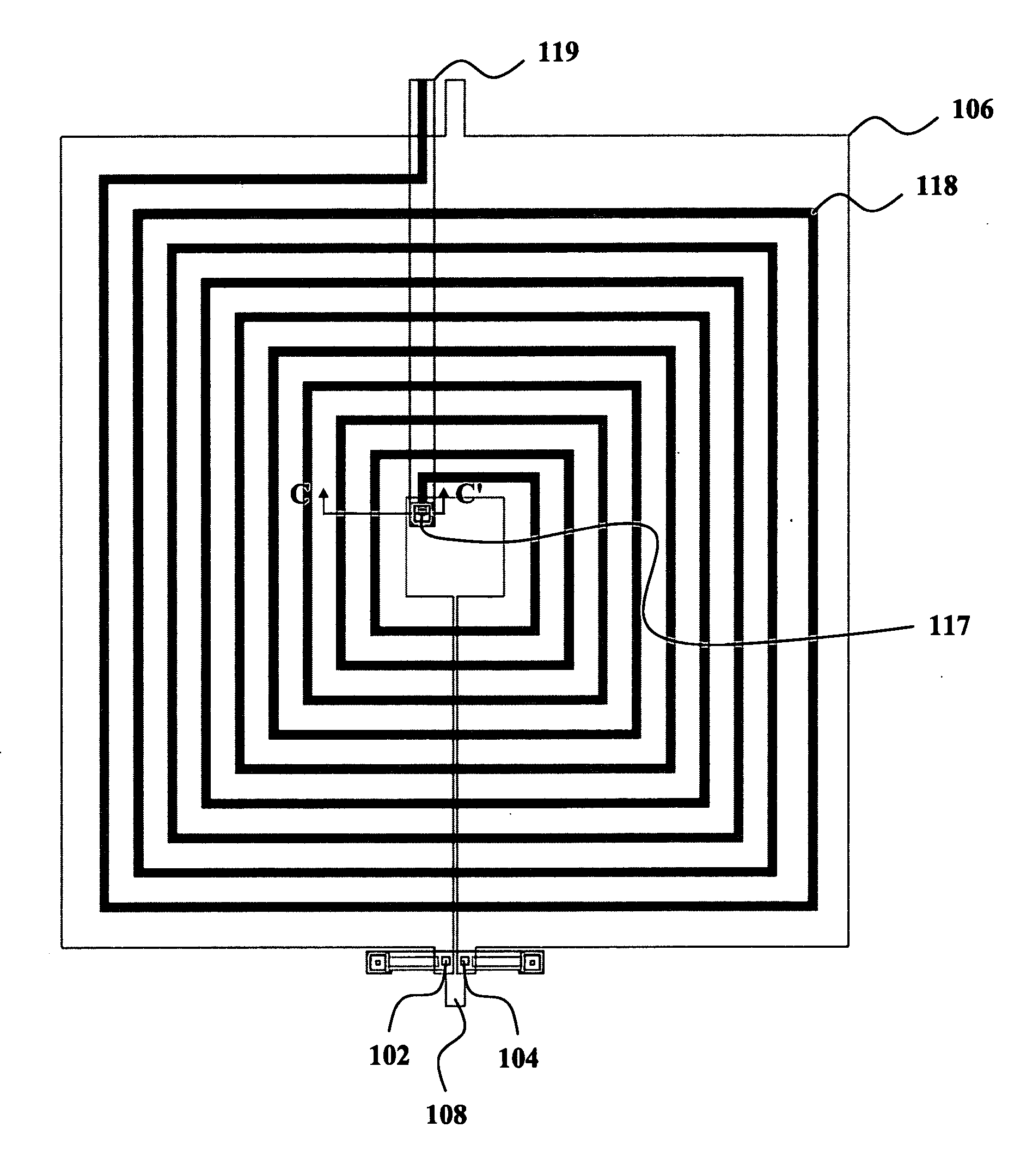
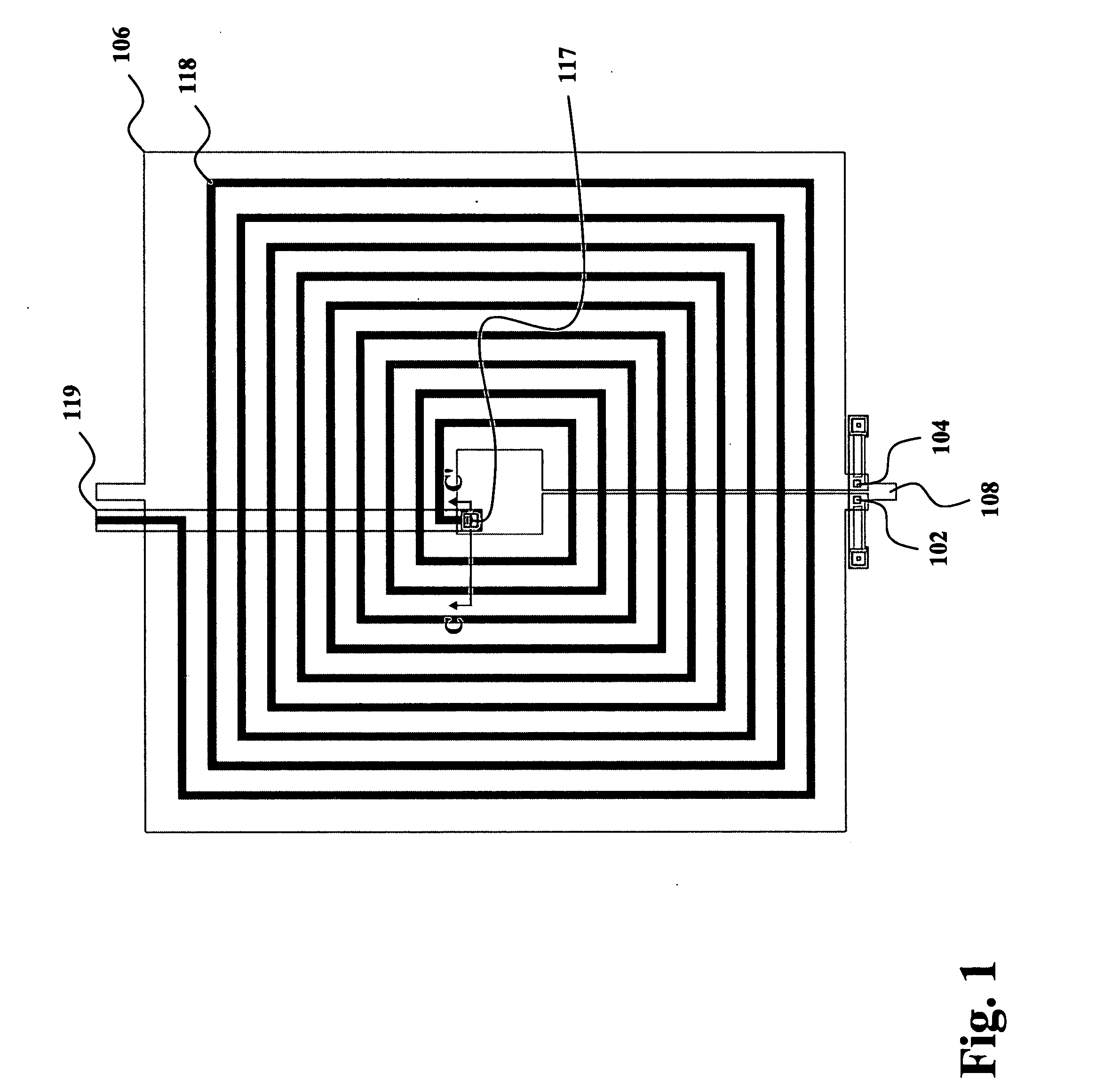
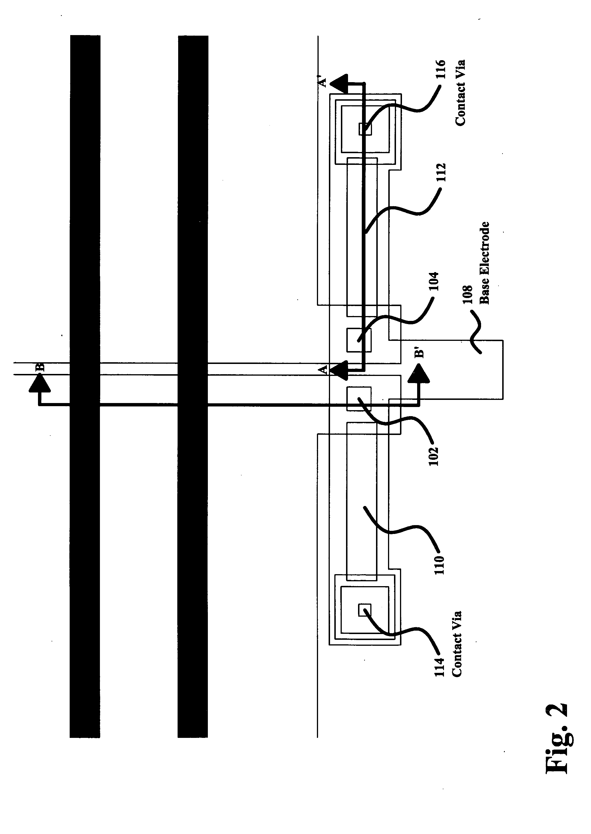
[0020] A direct current (dc) SQUID consists of two resistively-shunted Josephson junctions which are connected in parallel within a superconducting loop and biased by an external dc source. The SQUID may be current biased or voltage biased depending on the type of readout electronics used. Dc SQUIDs are typically multilayer thin-film devices, incorporating polycrystalline films of niobium for the Josephson junction electrodes. The element niobium is a borderline Type II superconductor with a relatively high critical temperature Tc=9.2 K and energy gap Δ≈1.5 millivolts (mV) which provide a reasonable temperature margin for junction operation at liquid h...


PUM

PropertyMeasurementUnit
Temperatureaaaaaaaaaa

Abstract

A Superconducting Quantum Interference Device (SQUID) is disclosed comprising a pair of resistively shunted Josephson junctions connected in parallel within a superconducting loop and biased by an external direct current (dc) source. The SQUID comprises a semiconductor substrate and at least one superconducting layer. The metal layer(s) are separated by or covered with a semiconductor material layer having the properties of a conductor at room temperature and the properties of an insulator at operating temperatures (generally less than 100 Kelvins). The properties of the semiconductor material layer greatly reduces the risk of electrostatic discharge that can damage the device during normal handling of the device at room temperature, while still providing the insulating properties desired to allow normal functioning of the device at its operating temperature. A method of manufacturing the SQUID device is also disclosed.

Description

CROSS-REFERENCE TO RELATED APPLICATION [0001] This is a non-provisional patent application of currently pending U.S. provisional patent application Ser. No. 60 / 513,747, filed Oct. 23, 2003, by Cantor et al., titled “Charge Dissipative Dielectric for Cryogenic Devices,” the entirety of which application is incorporated herein by reference.GOVERNMENT LICENSE RIGHTS [0002] The U.S. Government has a paid-up license in this invention and the right in limited circumstances to require the patent owner to license others on reasonable terms as provided for by the terms of Contracts NAS5-00236 and NAS5-00237, awarded by NASA.FIELD OF THE INVENTION [0003] This invention relates to Superconducting Quantum Interference Devices (SQUIDs) in general and more particularly to a process for the fabrication of thin film cryogenic devices which include a semiconductor layer that is conductive at room temperature and prevents electrostatic charge accumulation which can damage the device, but which is ins...

Claims


Application Information

Patent Timeline
IPC IPC(8): H01B1/00H01L
CPCG01R33/0052G01R33/035Y10S505/701H01L39/2493Y10S428/93H01L39/223H10N69/00H10N60/12H10N60/0912
Inventor CANTOR, ROBIN HAROLDHALL, JOHN ADDISON
Owner STAR CRYOELECTRONICS
Why Eureka
Try Eureka