Ultra-thin SOI mosfet method and structure

a technology of ultra-thin soi mosfet and mosfet, which is applied in the direction of semiconductor devices, basic electric elements, electrical equipment, etc., can solve the problem of limited lithography resolution and limit the scalability of the device, and achieve the effect of minimizing gate resistan

Inactive Publication Date: 2005-05-26
GLOBALFOUNDRIES INC
View PDF12 Cites 49 Cited by
  • Summary
  • Abstract
  • Description
  • Claims
  • Application Information

AI Technical Summary

Benefits of technology

[0012] A typical embodiment of the present inventive method employs triple chem-mech polishing and can be summarized as: (1) Employing a first Damascene process to form an isolation region, thereby defining the device's (MOSFET's) active area (AA); (2) Employing a second Damascene process is to form source / drain regions after an selective epitaxial growth; (3) Employing a third Damascene process form a fully self-aligned gate region where sidewall spacers are formed outside of the gate region, (i.e. within the source / drain regions), so that gate dimension can be precisely controlled by conventional lithographic techniques; (4) Performing silicidation in the source and drain region and sealing by means of a dielectric cap process so that source / drain and gate formation will not interfere with one other; (5) Forming relatively short gate poly, strapped by a conductive metal, to minimize gate resistance (a silicide gate structure is unnecessary).

Problems solved by technology

Gate sidewall spacers are formed outside of the gate area so that the scalability is limited solely by lithography resolution.

Method used


Image

  • Ultra-thin SOI mosfet method and structure
  • Ultra-thin SOI mosfet method and structure
  • Ultra-thin SOI mosfet method and structure

Examples


Embodiment Construction

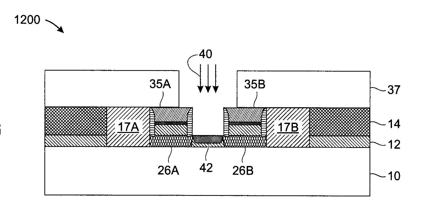
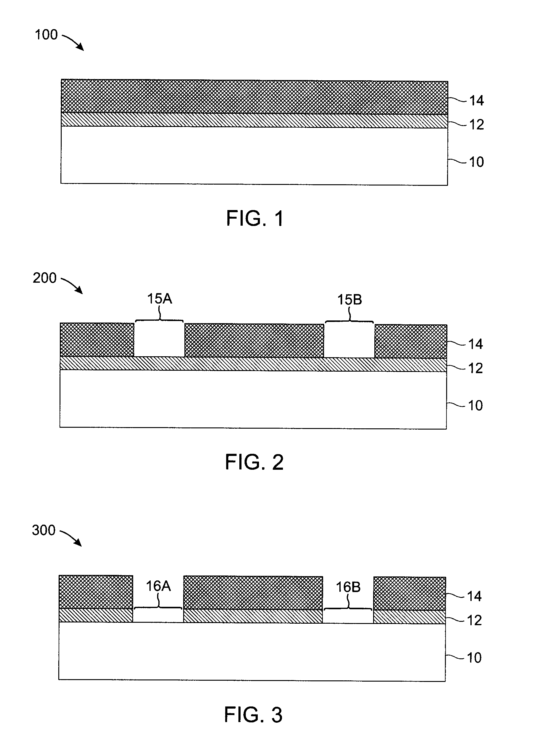
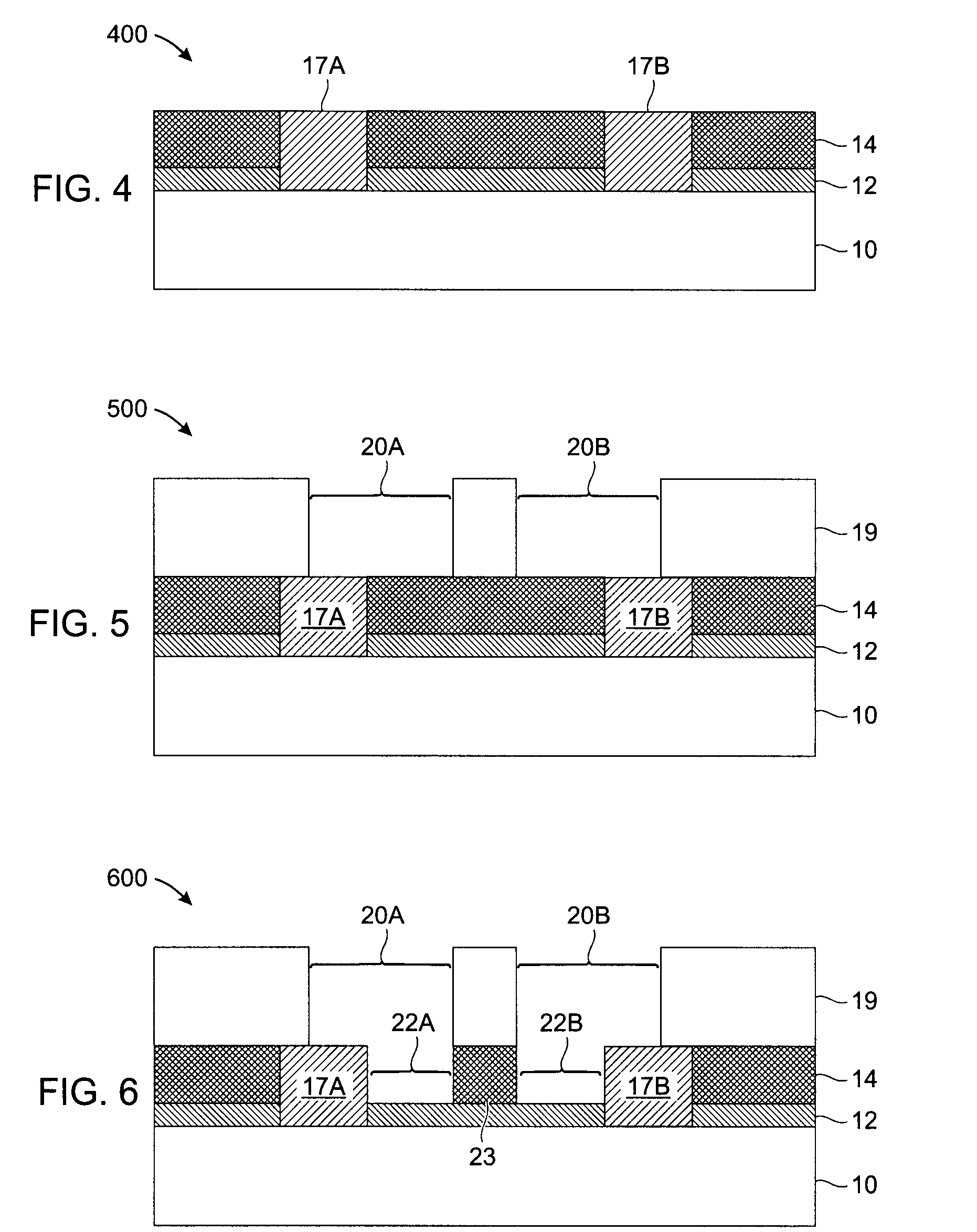
[0022] The present inventive technique produces raised source / drain junctions in MOS devices on a thin-SOI wafer with a robust isolation scheme by employing chem-mech polishing / planarization in combination with other processing techniques to form device isolation, source drain and gate structures in fully self-aligned fashion.

[0023] In a preferred embodiment of a method for forming a MOSFET device, triple chem-mech polishing is employed. This method can be summarized as: (1) Employing a first Damascene process to form an isolation region, thereby defining the device's (MOSFET's) active area (AA); (2) Employing a second Damascene process is to form source / drain regions after an selective epitaxial growth; (3) Employing a third Damascene process form a fully self-aligned gate region where sidewall spacers are formed outside of the gate region, (i.e. within the source / drain regions), so that gate dimension can be precisely controlled by conventional lithographic techniques; (4) Perfor...


PUM


Abstract

An ultra-thin, scaleable MOSFET transistor and fabrication method are described. The transistor features fully self-aligned, raised source / drain junctions on a thin SOI wafer and exhibits low contact resistance, low gate resistance and good device isolation characteristic. No extra lithographic mask steps are required beyond those required by conventional processes. The transistor is completely “bracketed” or surrounded by STI (shallow trench isolation), providing inherent isolation between it and any other devices on the SOI wafer. Gate sidewall spacers are formed outside of the gate area so that the scalability is limited solely by lithography resolution.

Description

BACKGROUND OF INVENTION [0001] The present invention relates to a semiconductor device, and more particularly to an ultra-thin, short-channel metal oxide semiconductor field effect transistor (MOSFET). [0002] In 1965, Dr. Gordon Moore, then Director of Research and Development for Fairchild Semiconductor, made the observation that the number of transistor devices per integrated circuit had been doubling every couple of years since the creation of the first integrated circuits in the late 1950's and that he expected the trend to continue for the foreseeable future. This observation was dubbed “Moore's Law” by the trade press. Now almost 40 years later, despite numerous dire predictions of fundamental obstacles, unrelenting industry efforts towards every-increasing semiconductor density have effectively affirmed Dr. Moore's prophetic observation, and the trend is still expected to continue unabated for the foreseeable future. The process of reducing semiconductor device size to increa...

Claims


Application Information

Patent Timeline
Patent Type & Authority Applications(United States)
IPC IPC(8): H01L21/336H01L21/762H01L29/45
CPCH01L21/76283H01L29/66772H01L29/66545H01L29/458
Inventor HSU, LOUISRADENS, CARL J.DIVAKARUNI, RAMACHANDRA
Owner GLOBALFOUNDRIES INC
Why Eureka
Try Eureka