
Multi-bit phase change memory cell and multi-bit phase change memory including the same, method of forming a multi-bit phase change memory, and method of programming a multi-bit phase change memory

Inactive Publication Date: 2005-05-26
IBM CORP
View PDF9 Cites 127 Cited by
  • Summary
  • Abstract
  • Description
  • Claims
  • Application Information

AI Technical Summary

Benefits of technology

[0011] Another aspect of the present invention is to provide a multi-bit memory cell having a simple structure with a minimal amount of wiring.
[0012] Another aspect of the present invention is to provide a multi-bit memory cell that can be easily and reliably programmed.

Problems solved by technology

Conventional nonvolatile multilevel memories have many disadvantages, particularly at the circuit and architectural levels.
The conventional multilevel approaches also have penalties on sensing speed, control complexity, and reliability.

Method used


Image

  • Multi-bit phase change memory cell and multi-bit phase change memory including the same, method of forming a multi-bit phase change memory, and method of programming a multi-bit phase change memory
  • Multi-bit phase change memory cell and multi-bit phase change memory including the same, method of forming a multi-bit phase change memory, and method of programming a multi-bit phase change memory
  • Multi-bit phase change memory cell and multi-bit phase change memory including the same, method of forming a multi-bit phase change memory, and method of programming a multi-bit phase change memory

Examples


Embodiment Construction

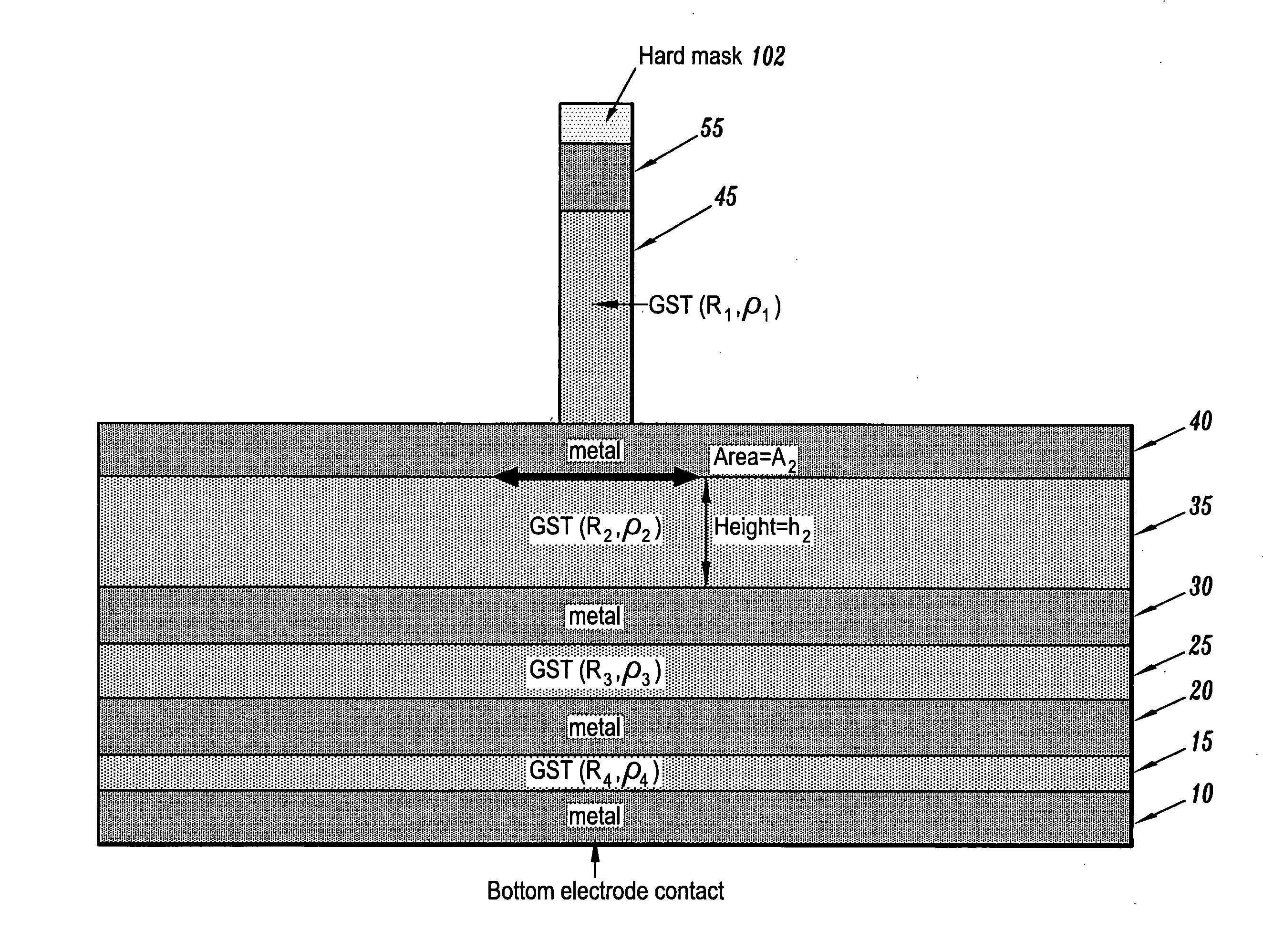
[0025] In various exemplary embodiments, the multi-bit memory cell according to the invention includes 2n phase change material layers, where n is the number of bits per cell. Conductive layers are disposed at the top and bottom of the cell and between individual phase change material layers. Multi-bit storage in the memory cell is obtained by crystallizing various phase change material layers. The phase change material layers can be crystallized by resistive heating of the phase change material layers.

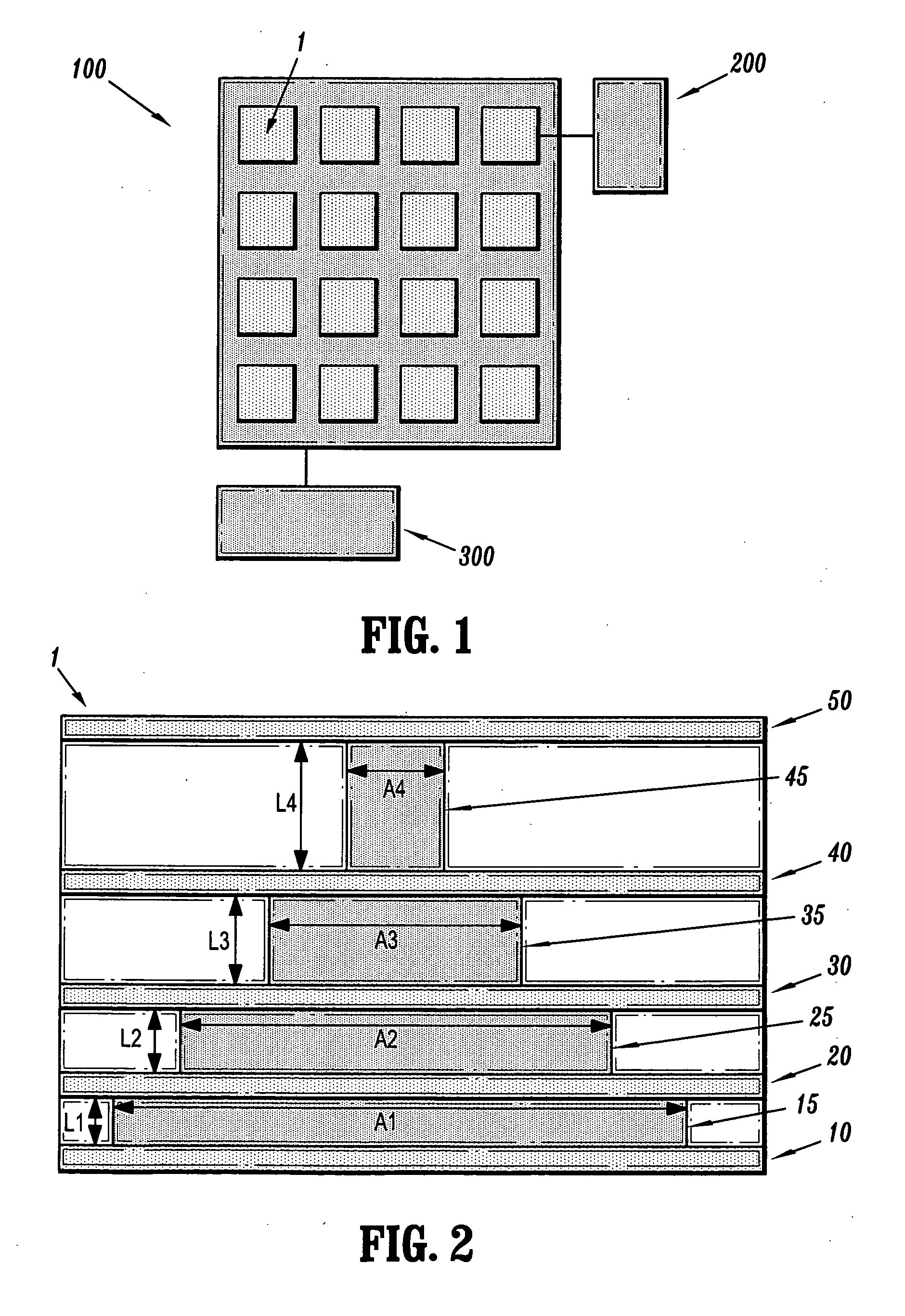
[0026]FIG. 1 shows a multi-bit phase change memory 100 according to an exemplary embodiment of the invention. The multi-bit phase change memory includes a plurality of phase change memory cells 1 arranged in an array, a programming circuit 200, and a sensing circuit 300.

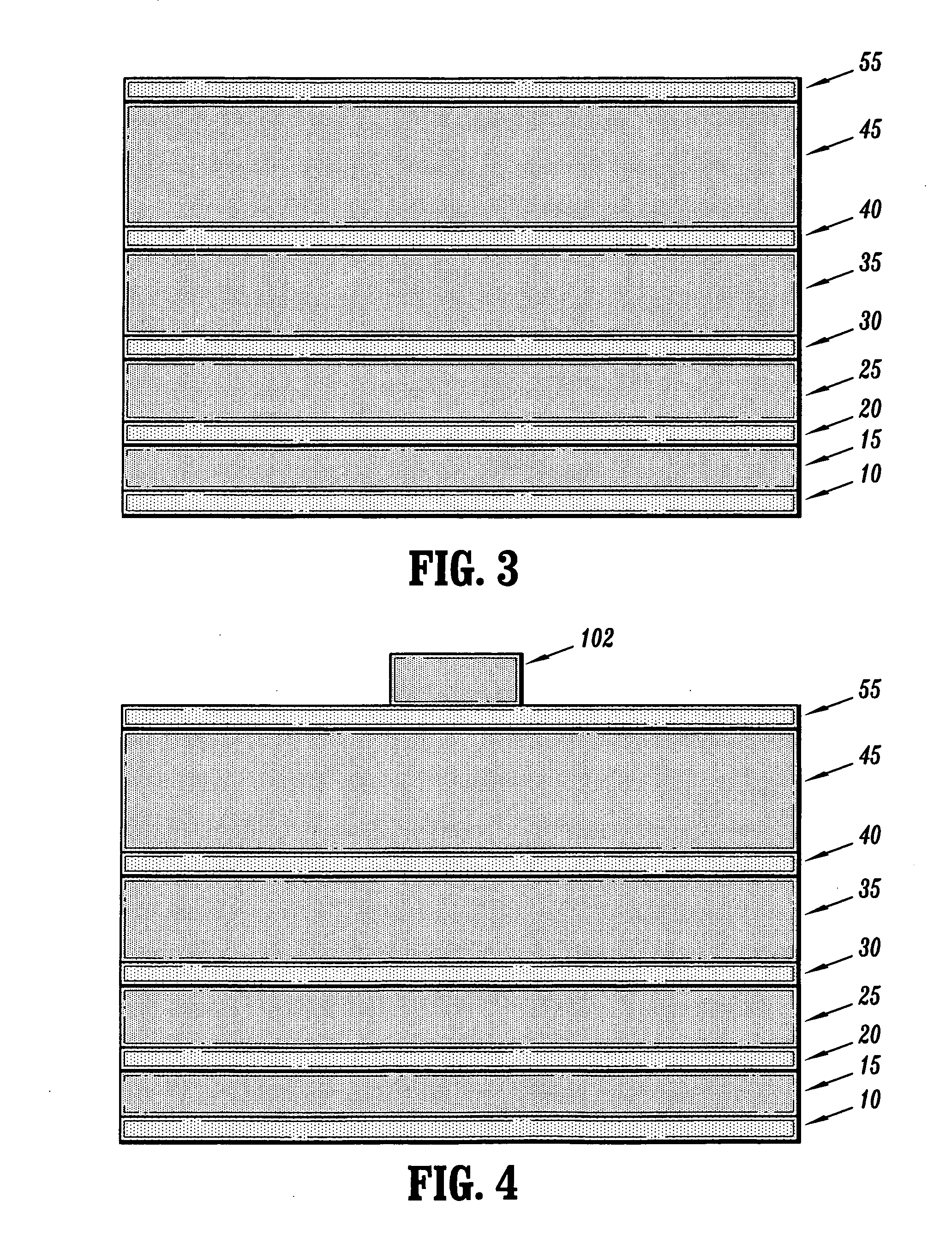
[0027]FIG. 2 is a cross-sectional view of a multi-bit memory cell used in the multi-bit phase change memory 100 according to an exemplary embodiment of the invention. The multi-bit memory cell 1 includes first throug...


PUM

PropertyMeasurementUnit
Electrical resistanceaaaaaaaaaa
Currentaaaaaaaaaa
Electrical conductoraaaaaaaaaa

Abstract

A multi-bit phase change memory cell including a stack of a plurality of conductive layers and a plurality of phase change material layers, each of the phase change material layers disposed between a corresponding pair of conductive layers and having electrical resistances that are different from one another.

Description

BACKGROUND OF THE INVENTION [0001] 1. Field of the Invention [0002] The present invention relates to memory devices that can store more than one bit per memory cell. [0003] 2. Description of the Related Art [0004] In conventional single-bit per cell memory devices, the memory cell assumes one of two information storage states, either an “on” state or an “off” state. This combination of either “on” or “off” defines one bit of information. A memory device using such single-bit cells to store n bits of data (n being an integer greater than 0) thus requires n separate memory cells. [0005] Increasing the number of bits which can be stored in a single-bit per cell memory device involves increasing the number of memory cells on a one-for-one basis with the number of bits of data to be stored. Methods for increasing the number of memory cells in a single memory device have relied upon advanced manufacturing techniques that produce larger chips containing more memory cells or that produce sm...

Claims


Application Information

Patent Timeline
IPC IPC(8): G11C11/56G11C16/02H01L21/311H01L27/24H01L45/00
CPCG11C11/56G11C11/5678G11C13/0004G11C2213/71H01L45/1675H01L45/06H01L45/1233H01L45/144H01L27/2463H10B63/80H10N70/231H10N70/826H10N70/8828H10N70/063
Inventor HAMANN, HENDRIK F.LAM, CHUNG HONSTEEN, MICHELLE LEIGHWONG, HON-SUM PHILIP
Owner IBM CORP
Features
  • Generate Ideas
  • Intellectual Property
  • Life Sciences
  • Materials
  • Tech Scout
  • Unparalleled Data Quality
  • Higher Quality Content
  • 60% Fewer Hallucinations
Learn More