

Color filter on thin film transistor type liquid crystal display device and method of fabricating the same
- Summary
- Abstract
- Description
- Claims
- Application Information
AI Technical Summary
Benefits of technology
Problems solved by technology
Method used
Image

Examples
first embodiment
[0042]FIG. 4 is a schematic cross-sectional view of a COT type LCD device according to the present invention. As shown in FIG. 4, a liquid crystal panel “LP” for a COT type LCD device includes first and second substrates 200 and 250 facing each other. Array elements “AP” including a color filter layer and a TFT are formed on the first substrate 200 and a first alignment key 202 is formed in a peripheral portion of the first substrate 200. The first alignment key 202 may be formed of the same material and the same layer as the array elements AP. A common electrode 252 and an orientation film 254 are sequentially formed on the second substrate 250. In addition, a second alignment key 256 is formed in a peripheral portion of the second substrate 250. The orientation film 254 may be formed using a printing method or an inkjet method.
[0043] When the orientation film 254 is formed using a printing method, an orientation material, such as polyimide, is printed onto the second substrate 250...
second embodiment
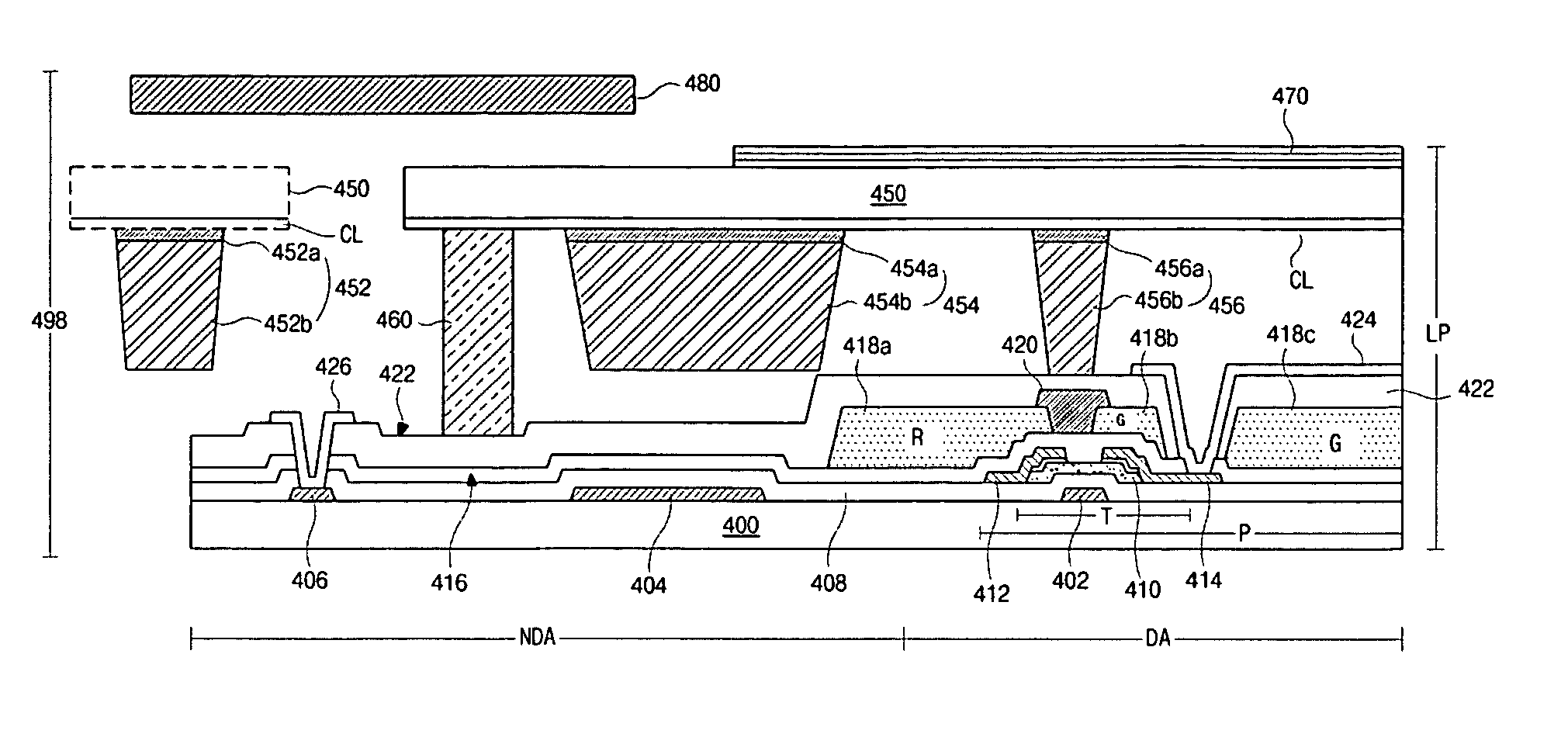
[0050]FIG. 6 is a schematic cross-sectional view of a COT type LCD device according to the present invention. As shown in FIG. 6, a COT type LCD device 498 includes a liquid crystal panel “LP” and a top case 480 surrounding the liquid crystal panel “LP.” The liquid crystal panel “LP” includes first and second substrates 400 and 450 attached with a sealant 460, and a polarization film 470 is formed on an outer surface of the second substrate 450. The liquid crystal panel “LP” has a display area “DA” used for displaying images and a non-display area “NDA” surrounding the display area “DA.” The display area “DA” includes a plurality of pixel regions “P” according to a size and a resolution of an LCD device.
[0051] A gate line 404 and a data line (not shown) crossing each other to define the pixel region “P” are formed on the first substrate 400. A thin film transistor (TFT) “T” including a gate electrode 402, an active layer 410, a source electrode 412 and a drain electrode 414 is conne...
third embodiment
[0064]FIG. 13 is a schematic cross-sectional view of a COT type LCD device according to the present invention. As shown in FIG. 13, a COT type LCD device 598 includes a liquid crystal panel “LP” and a top case 580 surrounding the liquid crystal panel “LP.” The liquid crystal panel “LP” includes first and second substrates 500 and 550 attached with a sealant 560, and a polarization film 570 is formed on an outer surface of the second substrate 550. The liquid crystal panel “LP” has a display area “DA” used for displaying images and a non-display area “NDA” surrounding the display area “DA.” The display area “DA” includes a plurality of pixel regions “P” according to a size and a resolution of an LCD device.
[0065] A gate line 504 and a data line (not shown) crossing each other to define the pixel region “P” are formed on the first substrate 500. A thin film transistor (TFT) “T” including a gate electrode 502, an active layer 510, a source electrode 512 and a drain electrode 514 is con...
PUM
 Abstract
Description
Claims
Application Information