
Nanoscopic wire-based devices and arrays

a wire-based device and array technology, applied in nanoelectromechanical switches, instruments, relays, etc., can solve the problems of preventing current designs from functioning reliably, and reducing the size limitation of silicon-based microelectronics, so as to achieve the fundamental physical limitations of both device elements and wire interconnects, and preventing current designs from being made small

Inactive Publication Date: 2005-06-02
PRESIDENT & FELLOWS OF HARVARD COLLEGE
View PDF36 Cites 60 Cited by
  • Summary
  • Abstract
  • Description
  • Claims
  • Application Information

AI Technical Summary

Benefits of technology

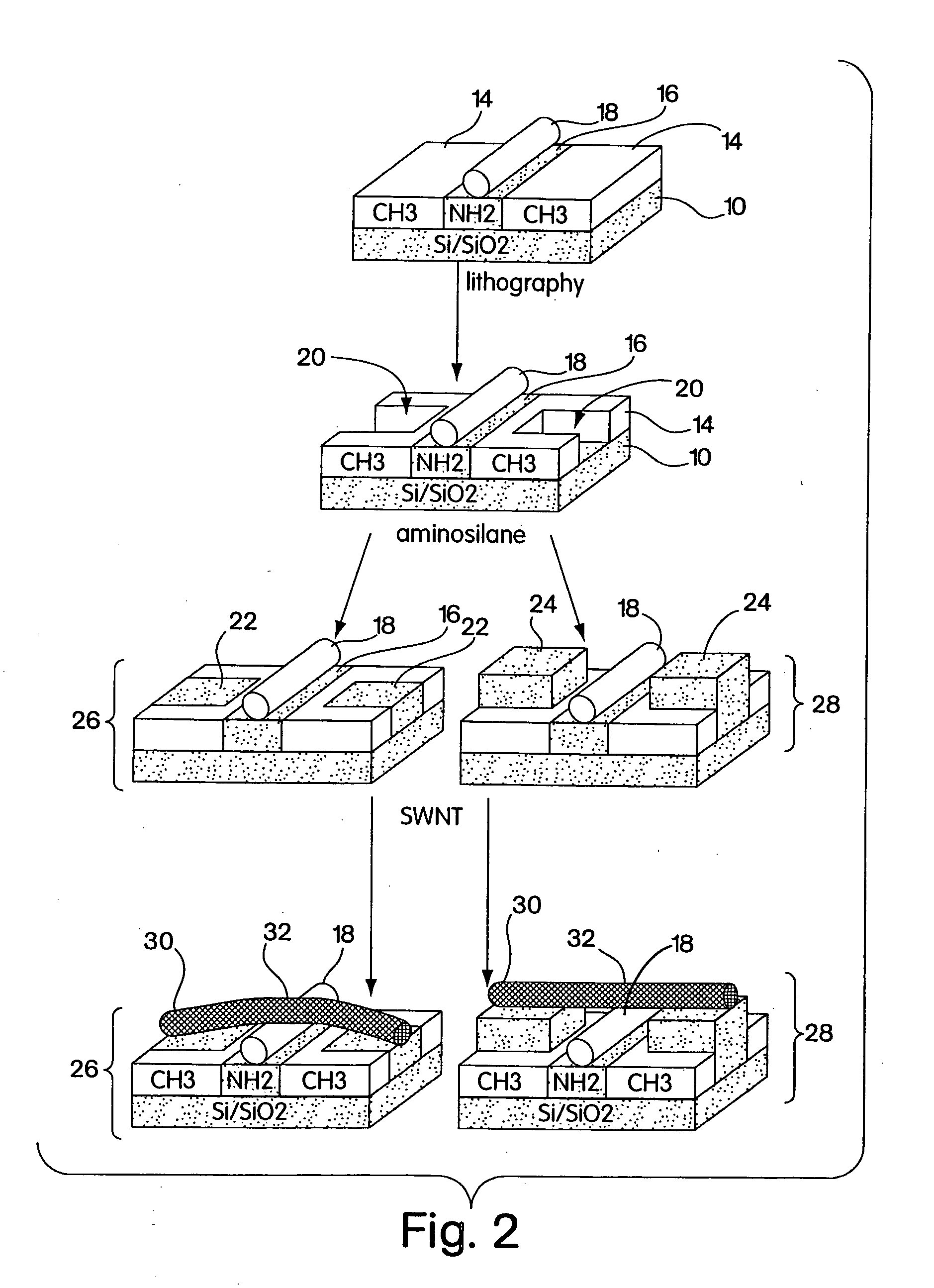
[0089] As noted above, it is a significant advantage of the invention that junction elements can be switched between “on” and “off” states remotely, i.e., by simply addressing at least one end of each of the wires that cross to form the memory element (wires 18 and 30 in FIGS. 2 and 4). Where the junction elements comprises memory elements, or diodes, some or preferably all of the memory elements are free of auxiliary circuitry defining the memory or diode elements and free of auxiliary circuitry addressing the memory or diode elements to switch them between states; the memory or diode element simply includes wires 18 and 30 that define the lead wires addressing the memory or diode element. Those of ordinary skill in the art will understand the meaning of auxiliary circuitry for switching a memory or diode element between “on” and “off” states, auxiliary circuitry defining memory states themselves, and the meaning of a device free of these components. An example of auxiliary circuitry defining memory states themselves includes an electrical pathway connecting two crossed conductors at a junction that can be switched from a conducting state to a non-conducting state. An example of auxiliary circuitry for switching a memory element between states includes circuitry connected to the electrical pathway that can be switched to render the pathway conducting or non-conducting.
[0090] One feature of the invention is that, with reference to FIG. 2, nanoscopic-scale wires 18 and 30 need not each be flexible nanoscopic wires such as nanotubes. As can be seen from the illustration and description relating to FIGS. 4 and 5, memory elements of the invention each include one wire (wire 18 in FIGS. 4 and 5) that need not move during switching, and can be made of essentially any material having appropriate conductivity that can be formed in the appropriate dimensions. Although nanotubes and other nanoscopic wires can be used for fixed wires 18, wires formed by more conventional techniques such as lithography can be used as well. Wire 30 should be selected to meet the additional requirement of repeated flexure during switching between “off” and “on” states, as illustrated. Wire 30 should thus be selected to have elasticity and robustness to meet this demand. Nanotubes exhibit such robustness and are ideal for use as flexing wires 30 in the invention. Thus, devices of the invention can be constructed entirely by directed assembly of pre-formed wires onto a surface or entirely from directed growth of wires at a surface, or a combination, or fixed wires 18 can first be formed via a conventional technique such as lithography followed by placement of flexing wires 30 by directed assembly, or directed growth.
[0091] Referring now to FIG. 7, a cut away schematic illustration of a crossbar array 80 of the invention is presented. Array 80 includes a series of parallel, equally-spaced wires 82, 84, 86, 88 . . . , and a series of parallel, equally-spaced wires 100, 102, 104, 106 . . . that cross (are perpendicular to) wires 82, 84 . . . . Each of wires 82, 84, 86 . . . is addressed by an electrode 120, 122, 124 . . . at one end thereof and each of wires 100, 102, 104, 106 . . . is addressed by an electrode 140, 142, 144 . . . at one end thereof. It is a feature of the invention that wires 82, 84, 86 . . . and wires 100, 102, 104 . . . require electrical contact with only one electrode, i.e., one interconnect can be used to address many individual junctions. Electrodes can be provided at opposite ends of the wires from those ends at which electrodes are shown (opposite ends not shown in FIG. 7), but this is optional. Each of wires 82, 84, 86 . . . crosses each of wires 100, 102, 104 . . . , each crossed wire junction defining a memory element as illustrated in FIGS. 2, 4, and 5 and discussed above. For example, junction 160 is a memory element defining the intersection of wires 88 and 104. When device 80 is constructed of memory elements as illustrated in arrangement 28 of FIG. 2, and in FIG. 4, at mechanical equilibrium wires 88 and 104 are free of contact and element 160 is “off”. Biasing electrodes 126 and 144 at opposite polarity brings wires 88 and104, at junction 160, into contact with each other (stable Van der Waals contact) and junction 160 is switched “on”. Bias need not be maintained between electrodes 126 and 144 to maintain element 160 in the “on” state in preferred embodiments. To switch element 160“off”, electrodes 126 and 144 are biased with the same polarity to repel wires 88 and 104 from each other at junction 160. Where device 80 includes junctions as illustrated in arrangement 26 of FIG. 2 and FIG. 5, at mechanical equilibrium junction 160 is in the “on” state with wires 88 and 104 contacting each other, and element 160 is switched “off” by biasing electrodes 126 and 144 at similar polarity. Switching element 160 back “on” is accomplished by biasing electrodes 126 and 144 at opposite polarity.
[0092] Another aspect of the present invention provides an article comprising an electrical crossbar array comprising at least two crossed nanoscopic wires defining a memory element capable of being switched irreversibly between at least two readable states. Thus, the device is “read-only”. In another embodiment, the article comprises an electrical crossbar array comprising at least two crossed nanoscopic wires defining a memory element capable of being switched reversibly. Thus, the devices can be used for a volatile RAM (e.g. require a power supply to keep the stored information) or a non-volatile RAM.

Problems solved by technology

Silicon-based microelectronics, however, can be made only so small.
That is, there is a size limitation smaller than which silicon-based microelectronics cannot be fabricated.
First, fundamental physical limitations will be reached for both device elements and wire interconnects that will prevent current designs from functioning reliably.
Second, the concurrent exponential increase in fabrication (FAB) facility cost is expected to make it uneconomical to consider increasing integration levels further (using silicon technology) even if it is physically meaningful.

Method used


Image

  • Nanoscopic wire-based devices and arrays
  • Nanoscopic wire-based devices and arrays
  • Nanoscopic wire-based devices and arrays

Examples


example 1

[0093] To quantify the bistability and switching behavior of the device element a total energy, ET, can be calculated:

ET=Evdw+Eelas+Eelec   (1)

where Evdw is the van der Waals (vdW) energy, Eelas is the elastic energy and Eelec is the electrostatic energy for the device. The first two terms in (1), which define the static potential, can be evaluated to assess the range of parameters that yield bistable devices. FIG. 11 shows plots of energy, ET=EvdW+Eelas, for a single 20 nm device as a function of separation at the junction. The series of curves correspond to initial separations of 0.8, 1.0, 1.2, 1.4, 1.6, 1.8, 2.0, 2.2, 2.4 nm for carbon nanotubes, with two well-defined minima observed for initial separations of 1.0 to 2.0 nm. These minima correspond to the crossing nanotubes being separated (2.4 nm) and in vdW contact (0.8 nm). The vdW interaction between nanotubes can be calculated by pairwise summation of a Lennard-Jones potential that has been shown previously to provide goo...

example 2

[0095] The effectiveness of switching the suspended nanotube devices between on and off states has been assessed by evaluating the voltage-dependent contribution of the electrostatic energy to the total energy. In this calculation, the boundary element method was used to numerically solve the Laplace equation for the complex three-dimensional geometry of the crossed nanotube device. Calculations of ET for switching a 20 nm device on and off (FIG. 15) demonstrate that it is possible to change reversibly between the on / off states using moderate voltages, which do not exceed the threshold field for nanotube failure. The switching voltages vary depending on the specific device geometry (i.e., shape of the static potential), and thus can be further optimized. For example, by using a thinner dielectric layer (that is, 4 vs 20 nm SiO2) the on and off switching thresholds can be reduced from 4.5 and 20 V to 3 and 5 V, respectively. The calculations also show that the electrostatic forces be...

example 3

[0097] Administration of reversible switching and the ability of the device to function as a non-volatile RAM is provided in this Example. Properties of suspended, crossed nanotube devices made from SWNT ropes were studied by mechanical manipulation (FIG. 16). Current-voltage (I-V) measurements made on the lower and upper nanotubes of a typical model device show ohmic behavior with resistances of 11 and 58 kΩ, respectively (FIG. 16A). The I-V curves between the upper and lower ropes in the off state were nonlinear, which is consistent with tunneling, with a resistance on the order of a GΩ. After switching on, the I-V curves exhibited ohmic behavior with a resistance of 112 kΩ (FIG. 16B). This large change in resistance is consistent with our predictions for off vs. on states in the suspended device architecture. Reversible switching between well-defined on / off states has also been observed in devices (FIG. 17). The smaller change in on / off resistances for the device in FIG. 17 is be...


PUM


Abstract

Electrical devices comprised of nanoscopic wires are described, along with methods of their manufacture and use. The nanoscopic wires can be nanotubes, preferably single-walled carbon nanotubes. They can be arranged in crossbar arrays using chemically patterned surfaces for direction, via chemical vapor deposition. Chemical vapor deposition also can be used to form nanotubes in arrays in the presence of directing electric fields, optionally in combination with self-assembled monolayer patterns. Bistable devices are described.

Description

RELATED APPLICATIONS [0001] This application is a continuation of International Patent Application Serial No. PCT / US00 / 18138, filed Jun. 30, 2000, which claims priority to U.S. Provisional Patent Application Ser. No. 60 / 142,216, filed Jul. 2, 1999.GOVERNMENT SPONSORSHIP [0002] This invention was sponsored by NIH Grant No. GM30367. The government has certain rights in the invention.FIELD OF THE INVENTION [0003] The present invention relates generally to the controlled formation and / or orientation of large molecules, such as nanotubes, on surfaces, and more particularly to formation of carbon nanotubes on surfaces for making nanoscopic-scale electronic devices such as memory arrays, configurable logic and other computer elements. BACKGROUND OF THE INVENTION [0004] During the past several decades there has been a nearly constant exponential growth in the capabilities of silicon-based microelectronics leading, for example, to tremendous advances in our computational capabilities. Silico...

Claims


Application Information

Patent Timeline
Patent Type & Authority Applications(United States)
IPC IPC(8): B82B3/00B82B1/00G11C13/02G11C23/00H01H59/00H01L27/10H01L27/24H01L29/06H01L29/66H01L49/00H01L51/00H01L51/30
CPCB82Y10/00Y10S977/943B82Y30/00B82Y40/00G11C13/025G11C23/00G11C2213/16G11C2213/72G11C2213/77G11C2213/81H01H1/0094H01L27/10H01L27/285H01L51/0048H01L51/0052H01L51/0595Y10S977/762Y10S977/932Y10S977/75Y10S977/843Y10S977/936B82Y15/00H10K19/202H10K85/221H10K85/615H10K10/701
Inventor LIEBER, CHARLES M.RUECKES, THOMASJOSELEVICH, ERNESTOKIM, KEVIN
Owner PRESIDENT & FELLOWS OF HARVARD COLLEGE
Learn More