Method for fabricating laminated silicon gate electrode

a gate electrode and laminate technology, applied in the direction of basic electric elements, electrical equipment, semiconductor devices, etc., can solve the problems of difficult gate electrode fabrication in the art of integrated circuit fabrication to achieve enhanced performance and enhanced dimensional control, and achieve enhanced performance and dimensional control. , the effect of enhancing dimensional control

Inactive Publication Date: 2005-06-09
TAIWAN SEMICON MFG CO LTD
View PDF27 Cites 0 Cited by
  • Summary
  • Abstract
  • Description
  • Claims
  • Application Information

AI Technical Summary

Benefits of technology

[0013] A second object of the present invention is to provide a method in accord with the first object of the present invention, wherein the gate electrode is formed with enhanced dimensional control and enhanced performance.
[0016] The present invention provides a method for forming a gate electrode for use within an integrated circuit, wherein the gate electrode is formed with enhanced dimensional control and enhanced performance.
[0017] The present invention realizes the foregoing objects within the context of forming a silicon layer over a substrate, wherein the silicon layer may be employed for forming a gate electrode within an integrated circuit device. Within the present invention, the silicon layer comprises at least one sub-layer formed of a higher crystalline silicon material and at least one sub-layer formed of a lower crystalline silicon material. In addition, within the present invention, the lower crystalline silicon material is formed incident to a hydrogen containing material treatment of the higher crystalline silicon material. By employing within the context of the present the lower crystalline silicon material as at least either an upper layer or a lower layer within a gate electrode, the gate electrode is formed with enhanced dimensional control and enhanced performance within a microelectronic fabrication, since the lower crystalline silicon material provides a smoother surface with enhanced electrical properties.

Problems solved by technology

In that regard, it is often difficult in the art of integrated circuit fabrication to fabricate gate electrodes with enhanced dimensional control and enhanced performance.

Method used


Image

  • Method for fabricating laminated silicon gate electrode
  • Method for fabricating laminated silicon gate electrode
  • Method for fabricating laminated silicon gate electrode

Examples


Embodiment Construction

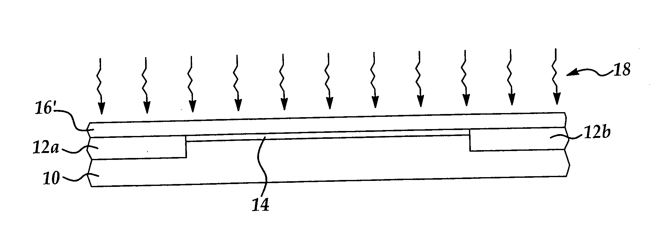
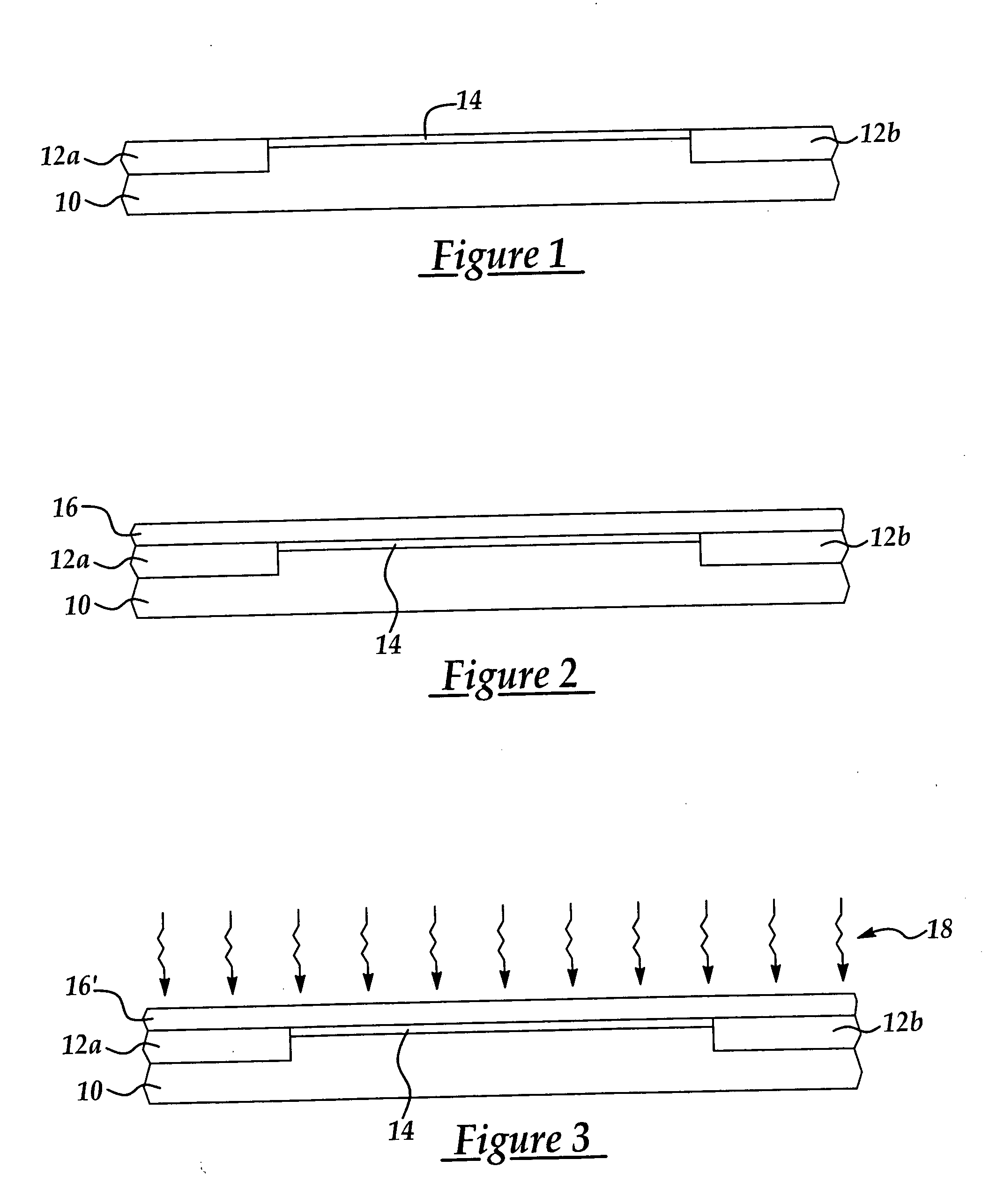
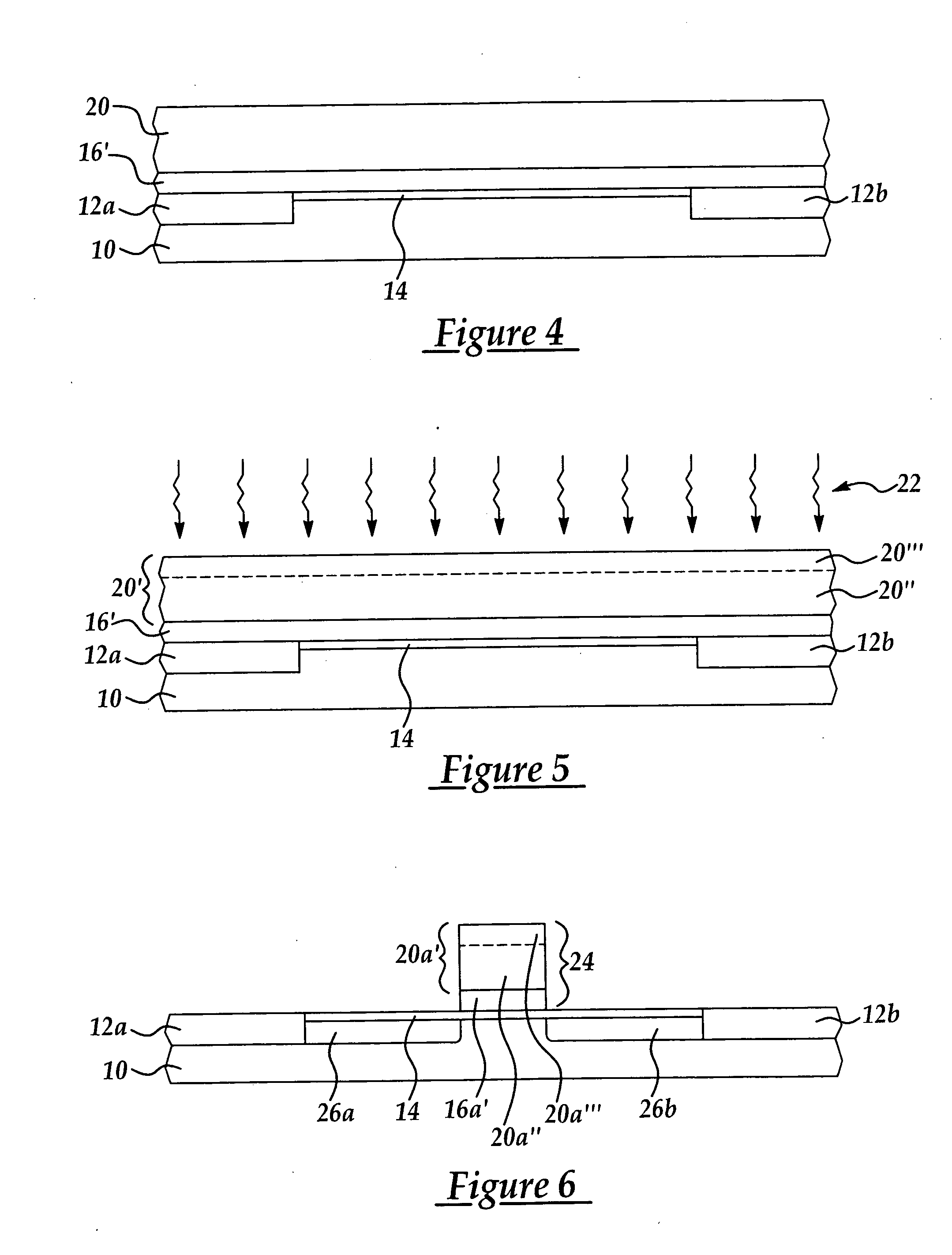
[0020] The present invention provides a method for forming a gate electrode for use within an integrated circuit, wherein the gate electrode is formed with enhanced dimensional control and enhanced performance.

[0021] The present invention realizes the foregoing objects within the context of forming a silicon layer over a substrate, wherein the silicon layer may be employed for forming a gate electrode within an integrated circuit device. Within the present invention, the silicon layer comprises at least one sub-layer formed of a higher crystalline silicon material and at least one sub-layer formed of a lower crystalline silicon material. In addition, within the present invention, the lower crystalline silicon material is formed incident to a hydrogen containing material treatment of the higher crystalline silicon material. By employing within the context of the present the lower crystalline silicon material as at least either an upper layer or a lower layer within a gate electrode,...


PUM

PropertyMeasurementUnit
thicknessaaaaaaaaaa
pressureaaaaaaaaaa
temperatureaaaaaaaaaa

Abstract

Within a method for forming a silicon layer, there is employed at least one sub-layer formed of a higher crystalline silicon material and at least one sub-layer formed of a lower crystalline silicon material. The lower crystalline silicon material is formed employing a hydrogen treatment of the higher crystalline silicon material. The method is particularly useful for forming polysilicon based gate electrodes with enhanced dimensional control and enhanced performance.

Description

BACKGROUND OF THE INVENTION [0001] 1. Field of the Invention [0002] The present invention relates generally to methods for fabricating microelectronic fabrications. More particularly, the present invention relates to methods for fabricating gate electrodes within field effect devices within semiconductor integrated circuit microelectronic fabrications. [0003] 2. Description of the Related Art [0004] Essential in the art of semiconductor integrated circuit microelectronic fabrication is the fabrication and use of field effect devices, such as field effect transistor (FET) devices. Field effect devices generally employ a gate electrode separated from a semiconductor substrate by a gate dielectric layer, to thus form a conductor / insulator / semiconductor capacitor, where charge carrier species concentrations are modulated within a channel region of the semiconductor substrate incident charge injection into the gate electrode. [0005] While gate electrodes are thus desirable in the art of ...

Claims


Application Information

Patent Timeline
Patent Type & Authority Applications(United States)
IPC IPC(8): H01L21/20H01L21/28H01L21/30H01L29/49H01L29/78
CPCH01L21/2022H01L21/28035H01L29/78H01L29/4925H01L21/3003H01L21/0262H01L21/02488H01L21/02532H01L21/02496H01L21/02505H01L21/0245H01L21/02381H01L21/02694H01L21/02595
Inventor CHEN, CHIA-LINYAO, LIANG-GICHEN, SHIH-CHANG
Owner TAIWAN SEMICON MFG CO LTD
Why Eureka
Try Eureka