Process for etching a SiN-based layer

a technology of silicon nitride and etching process, which is applied in the direction of semiconductor/solid-state device manufacturing, electric devices, transistors, etc., can solve the problems of significant deterioration of the performance of transistors, unintentional etching of the underlying layer of silicon, and incomplete etching of the layer of silicon nitride, so as to improve the selectivity and improve the etching effect of the layer

Active Publication Date: 2019-10-15
COMMISSARIAT A LENERGIE ATOMIQUE ET AUX ENERGIES ALTERNATIVES
View PDF9 Cites 0 Cited by
  • Summary
  • Abstract
  • Description
  • Claims
  • Application Information

AI Technical Summary

Benefits of technology

[0016]It has been noted that, in a particularly advantageous and unexpected manner, the method according to the present invention allows the layer containing SiN to be etched effectively without consuming other materials such as silicon or silicon dioxide. Moreover, this etching chemistry is particularly selective in the non-modified zones and portions of the layer containing SiN.
[0017]The invention thus allows the dimensional control to be considerably improved while not altering the underlying or neighbouring layers made of semiconductor or dielectric materials. The microelectronic devices manufactured according to the present invention thus have improved performance.
[0018]A step of etching, via plasma, the at least one modified zone using a chemistry comprising at least at least one compound chosen from SiwCl(2w+2) in addition to the compound comprising to the at least CxFz or CxHyFz provides particularly effective results in terms of etching selectivity.
[0023]In order to improve the selectivity of the etching of a layer containing SiN, a person skilled in the art would optionally plan to use a solution containing hydrofluoric acid (HF) and would attempt to modify the parameters of this etching. At best, a person skilled in the art would use hydrofluoric acid in vapour form. Optionally, a person skilled in the art would modify the pH of the hydrofluoric acid in order to improve the selectivity.

Problems solved by technology

One difficulty involves selectively etching the layer of silicon nitride in certain zones, typically outside of the sides of the gate, while preserving a thickness of silicon nitride in other zones, typically on the sides of the gate.
Indeed, during the etching of the silicon nitride, the current methods often lead to the incomplete etching of the layer of silicon nitride (this is called “under etching”) or the unintentional etching of the underlying layer of silicon (this is called “over etching”), typically forming a channel for the transistor.
Moreover, it is also difficult to selectively etch the silicon nitride with respect to the neighbouring layer of silicon oxide forming isolation trenches (usually called Shallow Trench Isolation (STI)) isolating the transistors, This unintentional consumption of silicon or of silicon oxide leads to significant deterioration of the performance of the transistor.
The various known solutions, inevitably lead to an often uncontrolled consumption of the underlying layers or to incomplete etching of the layer of silicon nitride.
This set of problems is even more important when transistors having different characteristics, for example n-type transistors and p-type transistors, must be manufactured on the same substrate and etching must take place on the transistors of one of these types while the transistors of the other type are already formed and are no longer protected.

Method used


Image

  • Process for etching a SiN-based layer
  • Process for etching a SiN-based layer
  • Process for etching a SiN-based layer

Examples


first embodiment

[0095]the present invention will be described in reference to FIGS. 1a to 1d. All the features, steps and advantages described in reference to these FIGS. 1a to 1d apply to all the other embodiments of the invention and in particular to those described in the other drawings.

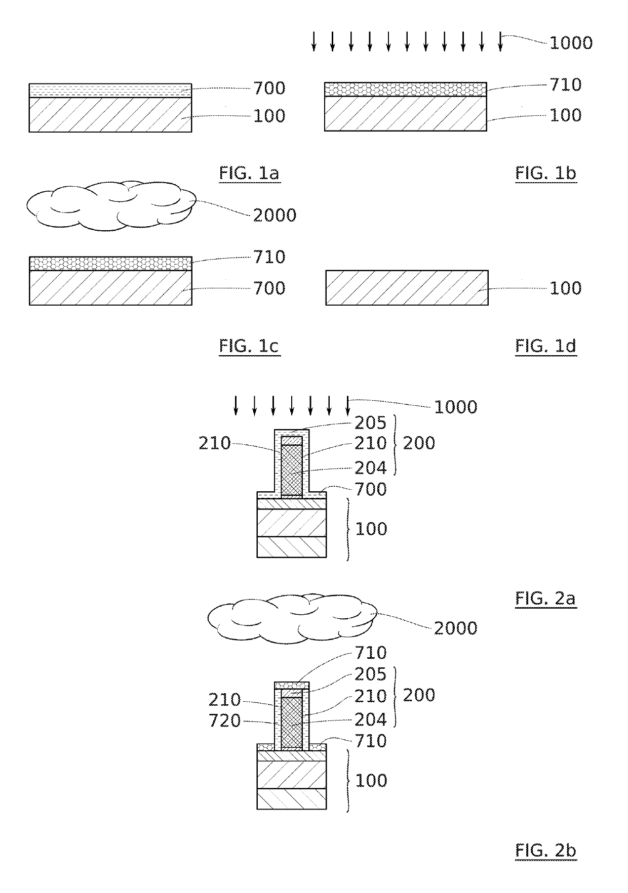
[0096]FIG. 1a illustrates a first step that involves providing a stack of layers comprising at least one substrate 100 above which there is a layer containing silicon nitride 700.

[0097]The substrate 100 can be a bulk single-layer substrate as illustrated in FIG. 1. Alternatively, the substrate 100 can be formed by a plurality of superimposed layers as illustrated in the examples of FIGS. 2a and 2b and 3a to 3h. The substrate 100, at its interface with the layer containing silicon nitride, is for example made from a semiconductor material preferably chosen from silicon (Si), germanium (Ge) and an alloy of silicon and germanium (SiGe). Alternatively, the substrate 100, at this interface, is made from an insulating ...

second embodiment

[0142]A second embodiment will now be described in reference to FIGS. 2a to 2b.

[0143]In this embodiment, the substrate 100 comprises a stack of layers. A pattern 200 is formed on the substrate 100. This pattern 200 is for example a transistor gate stack. Typically, this stack comprises at least successively starting from the substrate 100: an insulating layer forming a gate oxide, a gate 204 and a hard mask 205. The various layers forming such a pattern will be explained in detail in reference to FIG. 3a.

[0144]Before step 2a, a layer 700 containing silicon nitride is deposited on the pattern 200 and on the substrate 100. This deposition is conformal. The thickness of the layer 700 is therefore homogenous on the sides 210 of the pattern 200, on top of the pattern 200, and outside of the pattern 200.

[0145]Step 2a illustrates the modification of the layer 700 containing silicon nitride via the implantation 1000 of light ions. The implantation is anisotropic. The main direction of imp...

third embodiment

[0151]In reference to FIGS. 3a to 3h and 4, the invention will now be described.

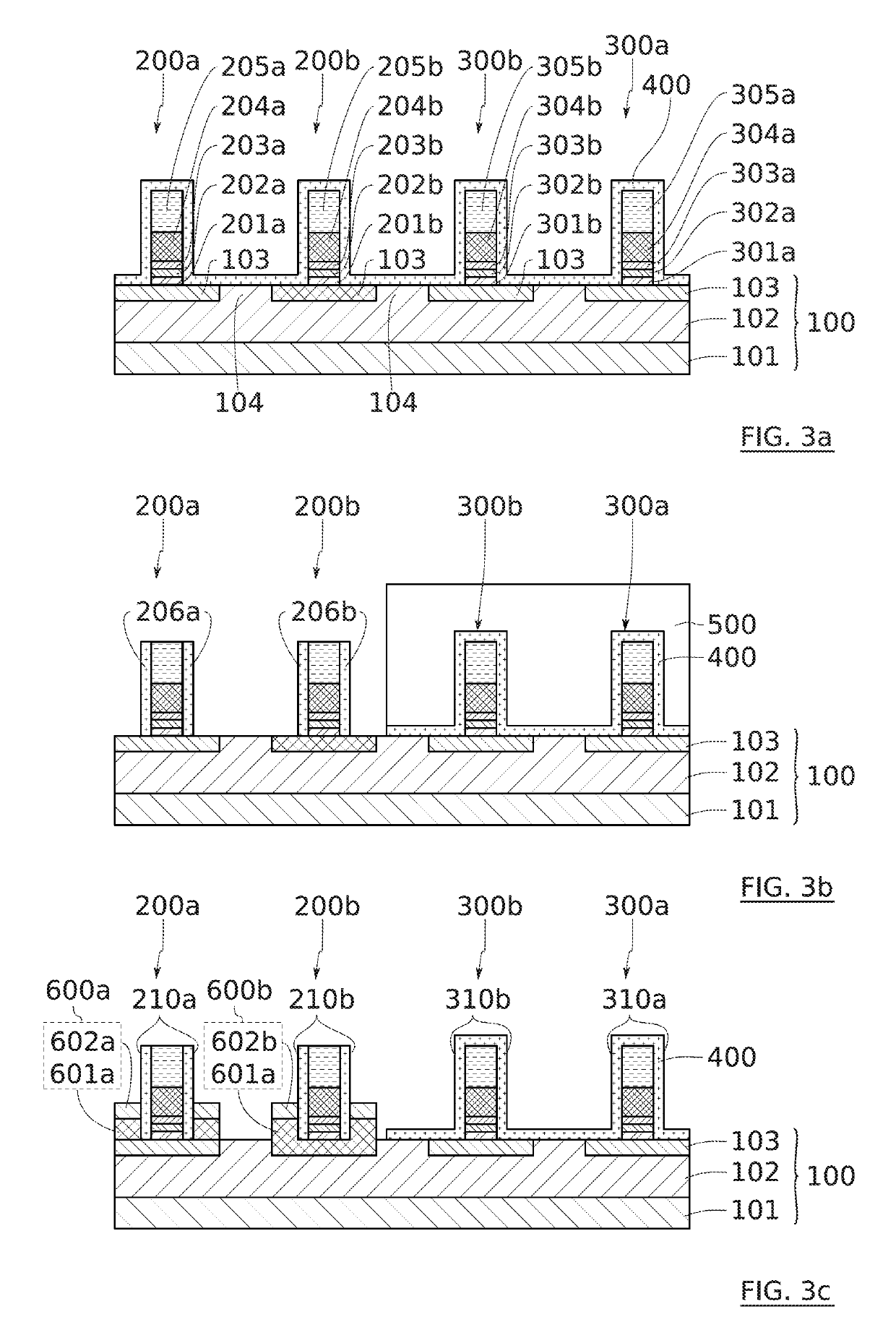
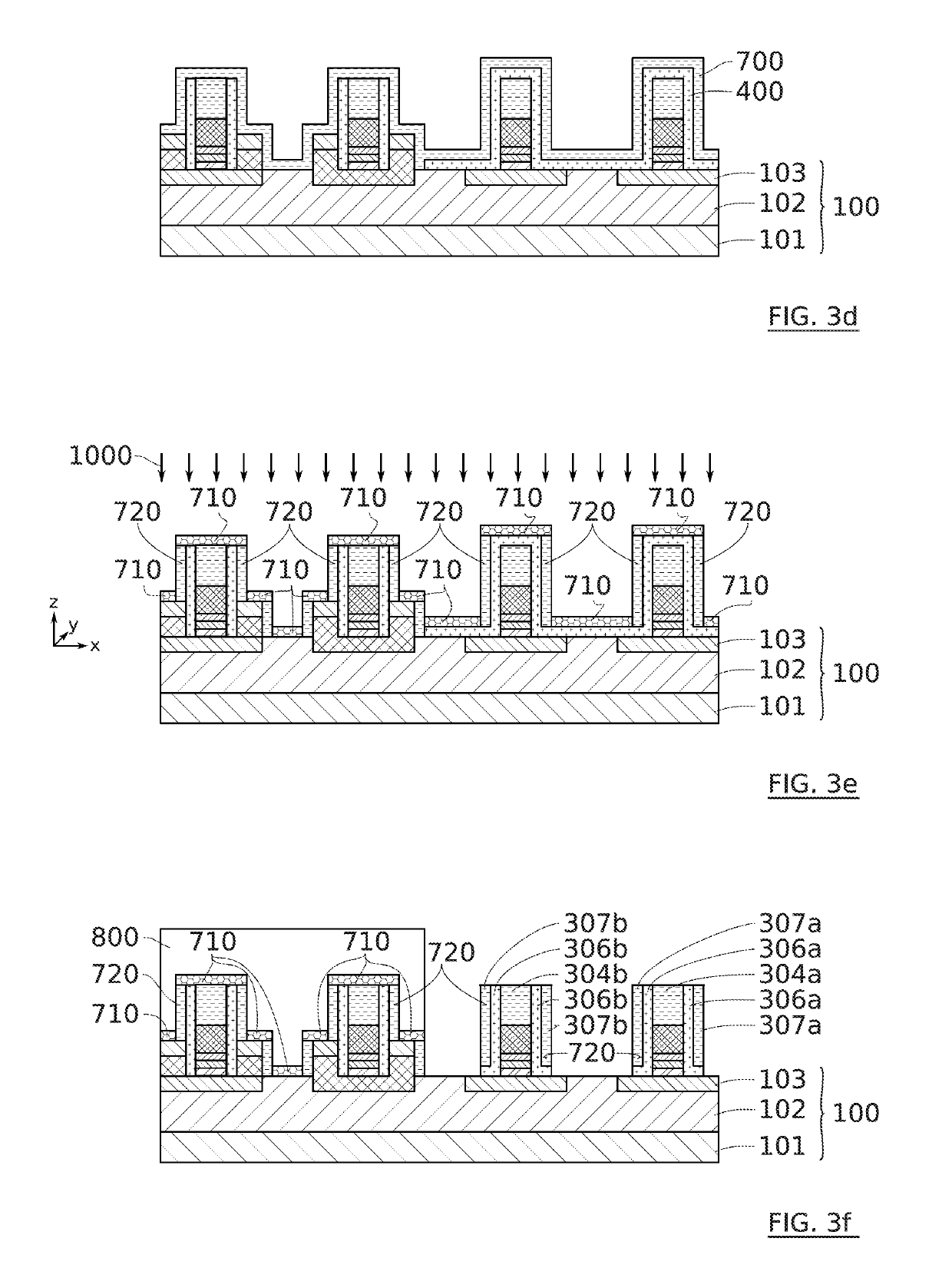
[0152]FIG. 3a illustrates a structure starting from which the steps of the method according to the invention are carried out. This structure comprises transistors in the process of being formed.

[0153]This structure comprises:[0154]an elaborate semiconductor on insulator (SOI) substrate 100. In the example illustrated, this elaborate substrate successively comprises a supporting layer 101; for example made of monocrystalline, polycrystalline or amorphous silicon; an insulating layer 102, usually called buried oxide (BOX for “Buried Oxide”) and an active semiconductor layer 103 intended to form a conductive channel of a transistor. The latter layer is for example made of silicon (Si), germanium (Ge) or silicon-germanium (SiGe), preferably monocrystalline.[0155]gate patterns 200a, 200b, 300a, 300b. As illustrated in FIGS. 3a to 3h, the semi conductor layer 103 is discontinuous in order to form disjointed po...


PUM


Abstract

A microelectronic method for etching a layer containing silicon nitride is provided, including the following successive steps: modifying the layer containing silicon nitride (SiN) so as to form at least one modified zone, the modifying including at least one implantation of ions made from hydrogen (H) in the layer containing SiN; and removing the at least one modified zone, the removing of the at least one modified zone including at least one step of etching of the at least one modified zone using a chemistry including at least: at least one compound chosen from the fluorocarbon compounds (CxFz) and the hydrofluorocarbon compounds (CxHyFz), and at least one compound chosen from SiwCl(2w+2) and SiwF(2w+2).

Description

TECHNICAL FIELD OF THE INVENTION[0001]The present invention relates in general to the techniques of etching a layer containing silicon nitride. It has a particularly advantageous but non-limiting use in the manufacturing, on the same substrate, of transistors having spacers containing silicon nitride and different characteristics, for example n-type or p-type doping or gate oxides having different thicknesses. It has an advantageous use in the manufacturing of such transistors on an FDSOI substrate.PRIOR ART[0002]Layers containing silicon nitride are widely used in numerous microelectronics devices and methods. In particular, this is the case for the manufacturing of gate spacers of transistors. One difficulty involves selectively etching the layer of silicon nitride in certain zones, typically outside of the sides of the gate, while preserving a thickness of silicon nitride in other zones, typically on the sides of the gate.[0003]Indeed, during the etching of the silicon nitride, t...

Claims


Application Information

Patent Timeline
Patent Type & Authority Patents(United States)
IPC IPC(8): H01L21/311H01L29/66H01L27/092H01L29/786H01L21/3115H01L21/84H01L21/8238
CPCH01L21/823807H01L21/823814H01L21/823864H01L21/84H01L21/31155H01L27/092H01L29/66742H01L29/66772H01L29/78618H01L29/78654H01L29/78684H01L21/31116H01L29/66
Inventor POSSEME, NICOLAS
Owner COMMISSARIAT A LENERGIE ATOMIQUE ET AUX ENERGIES ALTERNATIVES
Why Eureka
Try Eureka