Method for fabricating self-aligned contact hole

a contact hole and self-aligning technology, applied in the field of semiconductor devices, can solve the problems of reducing the area of the substrate exposed by the contact hole, and affecting the accuracy of conventional photolithography technology

Inactive Publication Date: 2009-07-07
DONGBU ELECTRONICS CO LTD
View PDF10 Cites 6 Cited by
  • Summary
  • Abstract
  • Description
  • Claims
  • Application Information

AI Technical Summary

Benefits of technology

[0009]It is, therefore, an object of the present invention to provide a method for fabricating a self-aligned contact hole in a semiconductor device, wherein an etching selectivity of an oxide to a nitride is improved so that an oxide layer can be effectively etched during the etching process for forming a self-aligned contact hole.
[0010]Another object of the present invention is to provide a method for fabricating a self-aligned contact hole in a semiconductor device, which enables increase of an overlap margin for a self-aligned contact in the semiconductor device.

Problems solved by technology

However, conventional photolithography technologies can sometimes fail to obtain sufficient accuracy for overlapping the variety of patterns with each other on a semiconductor substrate.
Because of such limitations of conventional photolithography technologies, a short circuit between conductive layers can occur during the process of forming a contact.
However, in the above conventional method for forming a self-aligned contact hole, an area of the substrate exposed by the contact hole can decrease because polymers (potentially a relatively large quantity) may disturb the etching process for forming the contact hole.
In this case, the nitride as well as the oxide can be etched so that the gate electrode pattern can be damaged.
In addition, increasing a thickness of the hard-mask nitride pattern for protecting the gate electrode pattern may result in increase of the aspect ratio of the contact hole.

Method used


Image

  • Method for fabricating self-aligned contact hole
  • Method for fabricating self-aligned contact hole
  • Method for fabricating self-aligned contact hole

Examples


Embodiment Construction

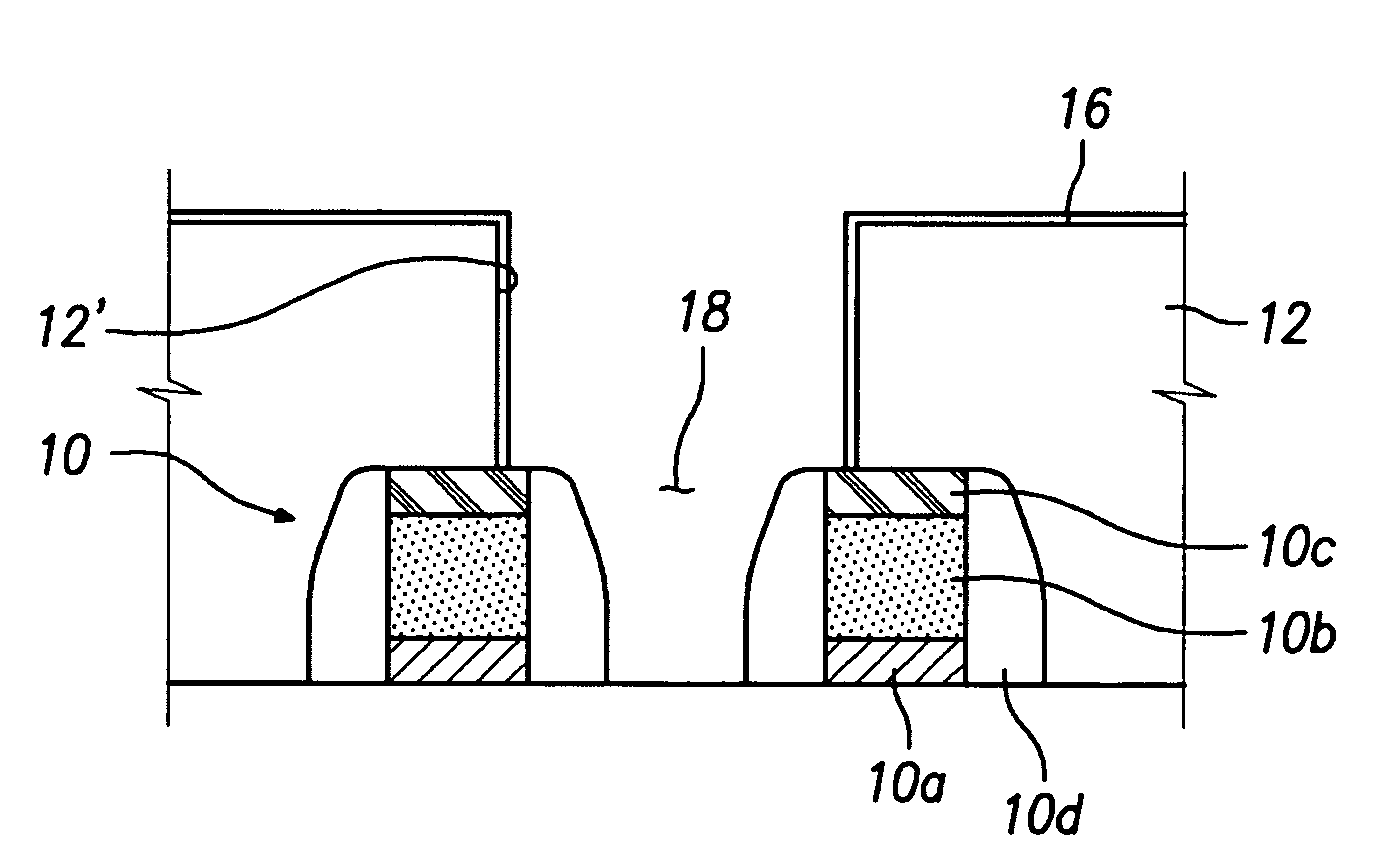
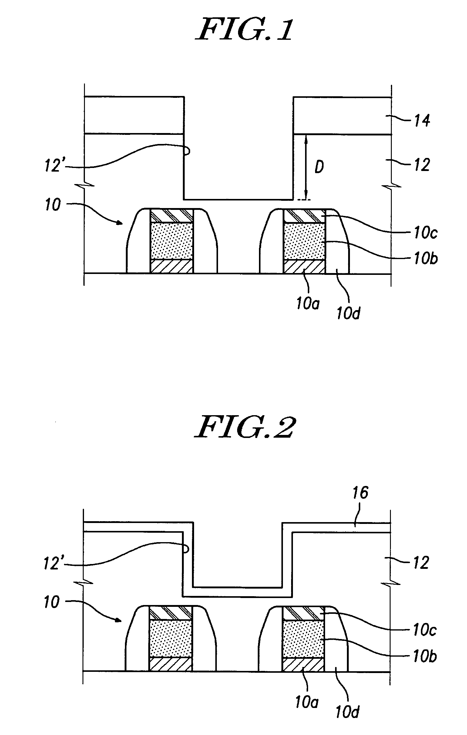
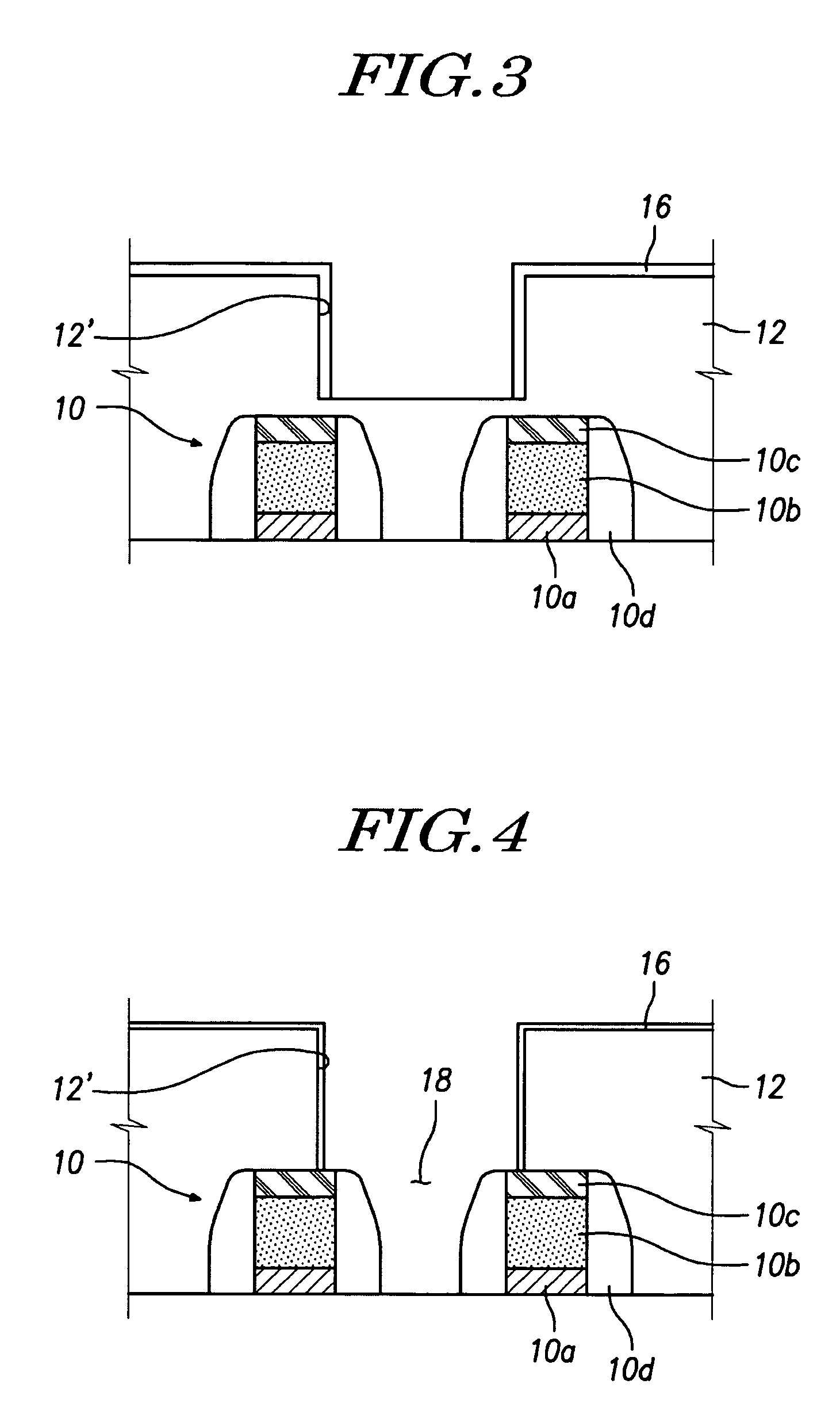
[0018]FIGS. 1 to 4 are cross-sectional views of a semiconductor device, illustrating an embodiment of a method for fabricating a self-aligned contact hole in a semiconductor device according to the present invention.

[0019]First, as shown in FIG. 1, a gate structure 10 is formed on a semiconductor substrate (not shown). Here, the gate structure 10 can be formed in such a manner known to those skilled in the art. Namely, a gate oxide layer, a gate electrode layer (e.g., a polysilicon layer), and a hard-mask nitride layer are formed in successive order. Then, these layers are patterned by a photolithography and etching processes so that a gate oxide pattern 10a, a gate electrode pattern 10b, and a hard-mask nitride pattern 10c are formed. Thereafter, another nitride layer (not shown) is deposited on the substrate and gate structures 10, then anisotropically etched (e.g., by dry and / or plasma etching) to form a nitride spacer 10d on sidewalls of the patterns 10a, 10b, and 10c.

[0020]Aft...


PUM


Abstract

Disclosed are: (i) a method for fabricating self-aligned contact hole in a semiconductor device, and (ii) a semiconductor device having a self-aligned contact. The method comprises the steps of: (a) forming an oxide layer covering a gate structure on a semiconductor substrate, the gate structure including a gate oxide pattern, a gate electrode pattern, a hard-mask nitride pattern, and a spacer nitride on sidewalls thereof; (b) forming a mask pattern on the oxide layer; (c) forming a contact trench by removing a portion of the oxide layer, exposed by the mask pattern, to a predetermined depth; (d) forming a buffer layer on the oxide layer, including in the contact trench; (e) etching a portion of the buffer layer at a bottom of the contact trench to expose a portion of the oxide layer; and (f) forming a contact hole by etching the exposed oxide layer using a remaining buffer layer as an etching mask.

Description

[0001]This application claims the benefit of Korean Application No. 10-2004-0111049, filed on Dec. 23, 2004, which is incorporated by reference herein in its entirety.BACKGROUND OF THE INVENTION[0002]1. Field of the Invention[0003]The present invention relates to a semiconductor device and a method for fabricating the same. More specifically, the present invention relates to a method for fabricating a self-aligned contact hole in a semiconductor device.[0004]2. Description of the Related Art[0005]As integration of semiconductor devices has increased, multilevel-interconnection has become an indispensable technology for manufacturing semiconductor devices. In multilevel-interconnection, a variety and / or plurality of miniaturized wiring patterns at different levels of the device generally overlap with each other on a plurality of dielectric layers. However, conventional photolithography technologies can sometimes fail to obtain sufficient accuracy for overlapping the variety of patter...

Claims


Application Information

Patent Timeline
Patent Type & Authority Patents(United States)
IPC IPC(8): H01L21/44
CPCH01L21/76897H01L21/28
Inventor HWANG, HAN GYOO
Owner DONGBU ELECTRONICS CO LTD
Why Eureka
Try Eureka