Apparatus for supporting substrate and plasma etching apparatus having the same

a technology of plasma etching apparatus and substrate, which is applied in the direction of coating, chemical vapor deposition coating, metallic material coating process, etc., can solve the problems of difficult to align the semi-conductor substrate, difficult to concentrate plasma onto the edge region of the substrate, and unsuitable layers or particles can be deposited on the edge region of the semiconductor substrate, so as to improve the etching capability of plasma and prevent damage to the central region of the substrate. , the effect of improving the central region

Inactive Publication Date: 2015-03-17
SOSUL
View PDF45 Cites 7 Cited by
  • Summary
  • Abstract
  • Description
  • Claims
  • Application Information

AI Technical Summary

Benefits of technology

[0060]As described above, since the heating units are disposed in the wall of the chamber and the substrate support to heat a substrate introduced into the chamber, the edge region of the substrate can be etched more efficiently.
[0061]Furthermore, the shield part is disposed around an edge region of a substrate, and the antenna for generating plasma is disposed outside the shield part. Since the antenna is disposed around a side of the edge region of the substrate, high-density plasma can be generated in the chamber, and the high-density plasma can be uniformed concentrated onto the edge region of the substrate by disposing the Faraday shield between the shield part and the antenna.
[0062]As described above, inert gas is injected to an upper region of a non-etch region of a substrate through a mask part which covers the non-etch region of the substrate. Therefore, penetration of process gas to the non-etch region of the substrate can be prevented, and thus patterns disposed on the non-etch region can be protected.
[0063]As described above, the substrate supporting apparatus and the substrate edge etching apparatus having the same provide the electrode supporting the substrate to the center of the body of the substrate support, and provides the electrode applying high frequency waves to the edge of the body to maintain substrate gripping force of the substrate support, improve etching capability using plasma on the substrate edge region, and prevent damage of the substrate central region caused by the plasma.
[0064]Also, the substrate supporting apparatus and the substrate edge etching apparatus having the same provide members for refrigerant and heating as well as members for high frequency waves and DC power to the central region of the body of the substrate support to minimize a change in the process condition on the edge region of the body.

Problems solved by technology

However, undesired layers or particles can be deposited on the edge region of the semiconductor substrate during manufacturing processes.
In addition, it may be difficult to align the semi-conductor substrate due to the undesired layers or particles.
However, it is difficult to concentrate plasma onto the edge region of the substrate since the electrode portion is disposed at the outer upper portion of the chamber.
Furthermore, since the density of the CCP is low (i.e., the etch rate of the conventional etching apparatus is low), it takes much time to remove undesired layers or particles from the edge region of the semiconductor substrate.
Moreover, some layers cannot be removed using the conventional etching apparatus.
In addition, due to a low process temperature, it is difficult to remove a metal layer from the edge region of the semiconductor substrate using the conventional etching apparatus.
Particularly, in a case where the electrostatic chuck is used for a substrate edge etching apparatus, plasma density on a substrate edge region is reduced, so that etching the substrate edge region is not efficiently performed, and a substrate central region, which is a non-etch region, is damaged by plasma.

Method used


Image

  • Apparatus for supporting substrate and plasma etching apparatus having the same
  • Apparatus for supporting substrate and plasma etching apparatus having the same
  • Apparatus for supporting substrate and plasma etching apparatus having the same

Examples


Embodiment Construction

[0085]Hereinafter, specific embodiments will be described in detail with reference to the accompanying drawings. The present invention may, however, be embodied in different forms and should not be construed as limited to the embodiments set forth herein. Rather, these embodiments are provided so that this disclosure will be thorough and complete, and will fully convey the scope of the present invention to those skilled in the art. In the figures, like reference numerals refer to like elements throughout.

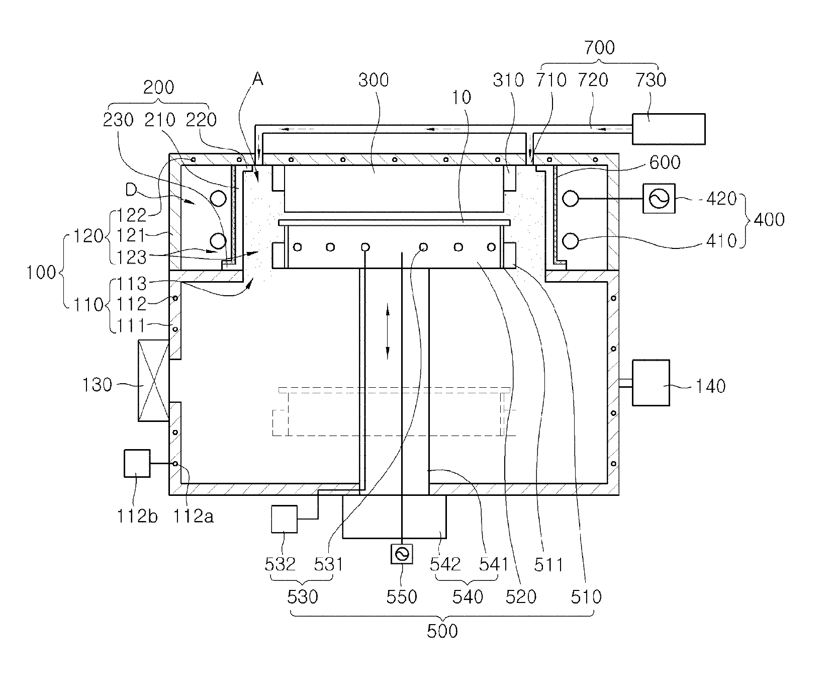
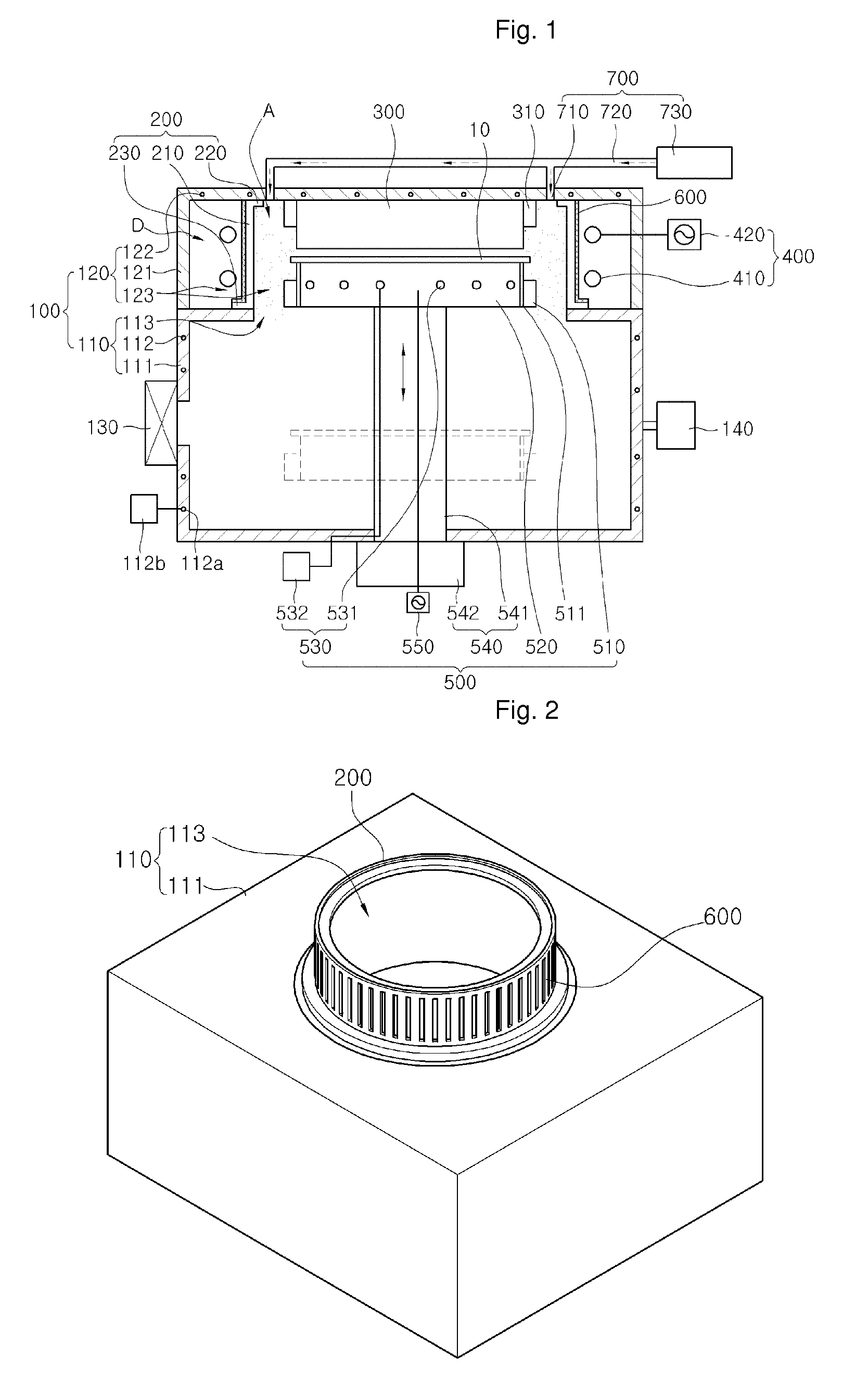
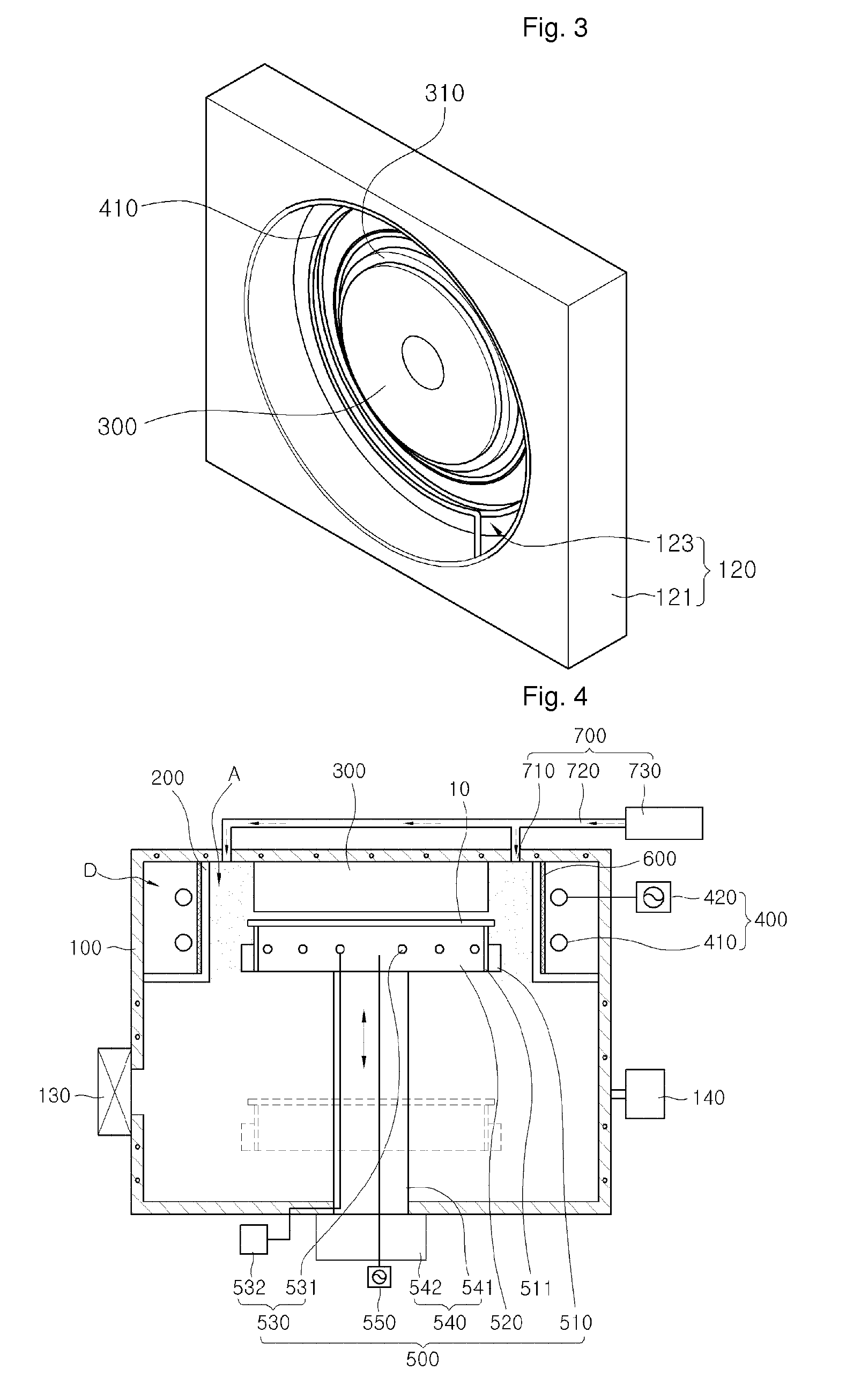
[0086]FIG. 1 is a schematic view illustrating a plasma etching apparatus in accordance with a first exemplary embodiment. FIG. 2 is a perspective view illustrating a lower chamber in accordance with the first exemplary embodiment, and FIG. 3 is a perspective view illustrating an upper chamber in accordance with the exemplary embodiment. FIGS. 4 and 5 are schematic views illustrating variants of the plasma etching apparatuses in accordance with the exemplary embodiments.

[0087]Referri...


PUM

PropertyMeasurementUnit
widthaaaaaaaaaa
distanceaaaaaaaaaa
distanceaaaaaaaaaa

Abstract

Provided are a substrate supporting apparatus and a plasma etching apparatus having the same. There is provided a substrate supporting apparatus that can separately provide powers to a central region and an edge region by disposing an electrode supporting a substrate at the central region of the substrate supporting apparatus, and disposing an electrode receiving radio frequency (RF) power at the edge region of the substrate supporting apparatus. There is provided a substrate edge etching apparatus having the substrate supporting apparatus for removing layers or particles deposited in an edge region of a semiconductor substrate and preventing damage of a center region of the semiconductor substrate during an etching process of the substrate edge.

Description

TECHNICAL FIELD[0001]The present disclosure relates to an apparatus for supporting a substrate and a plasma etching apparatus having the same, and more particularly, to a plasma etching apparatus that can separately provide powers to a central region and an edge region by disposing an electrode supporting a substrate at the central region of the substrate supporting apparatus, and disposing an electrode receiving radio frequency (RF) power at the edge region of the substrate supporting apparatus, so that thin layers or particles deposited in an edge region of the substrate can be removed using plasma.BACKGROUND ART[0002]Generally, devices or circuit patterns are not formed in an edge region of a semi-conductor substrate since the edge region is used for conveying the semiconductor substrate. However, undesired layers or particles can be deposited on the edge region of the semiconductor substrate during manufacturing processes. If the manufacturing processes are continued without rem...

Claims


Application Information

Patent Timeline
Patent Type & Authority Patents(United States)
IPC IPC(8): C23C16/00H01L21/306H01L21/67H01L21/683H01L21/687
CPCH01L21/67069H01L21/68742H01L21/6831
Inventor LEE, WON HAENGRHA, KWAN GOOLEE, JUNG HEEJANG, CHUL HEELEE, HYANG JOOKIM, DONG WAN
Owner SOSUL
Why Eureka
Try Eureka