Receiver optical subassembly

a technology of optical sub-assembly and receiver, which is applied in the direction of optical elements, instruments, optics, etc., can solve the problems of large package size, complicated package process, and complicated facilities and processes, and achieve effective alignment of optical transceiver elements, small size, and high performance

Inactive Publication Date: 2005-06-09
IND TECH RES INST
View PDF4 Cites 12 Cited by
  • Summary
  • Abstract
  • Description
  • Claims
  • Application Information

AI Technical Summary

Benefits of technology

[0008] The object of the invention is to provide a receiver optical subassembly having an integrated package and performing effective alignment of optical transceiver elements. The optical subassembly has high performance and small size.
[0009] A receiver optical subassembly for transforming received optical signal into electrical signal according to the invention includes a substrate, a photoreceiver and a transimpedance amplifier. There are high-speed traces formed on the substrate. The positive and negative pads of the photoreceiver are coplanar and connected to the traces through flip chip so as to reduce the parasitic impedance effect and improve the high-speed performance of the optical subassembly. The transimpedance amplifier is electrically connected to the traces via flip chip, wire bonding or other methods. The photoreceiver and the transimpedance amplifier are connected via the high-speed traces formed on the ceramic substrate.
[0010] The invention further includes a base and a metal case for packing aforesaid substrate, photoreceiver and transimpedance amplifier. The base includes a plurality of electrical pins including a ground pin. The substrate has grounding pad electrically connects with the ground pin for reducing crosstalk and other interferences generated by high frequency signals. The metal case and the base form a shield for the substrate, the photoreceiver and the transimpedance amplifier. The grounding pin connects to the metal case for good shielding. Electrical signals are connected outwards via the electrical pins passing through the bottom of the base.
[0011] In order to improve the coupling efficiency, the light-receiving surface of the photoreceiver is formed with a micro lens. In accompany with some external coupling elements, the beam coupling system is decreased with requirements of alignment precision and improved with coupling efficiency.

Problems solved by technology

The facilities and processes are rather complicated and time-consuming.
Because the optical fiber is located in an etched groove formed on the mount substrate, the precision of the groove greatly influences the alignment; also, the package gets a larger size, and the package process is more complicated.
Because the manufacturing process influences the construction and alignment precision of an optical subassembly, in order to improve the quality and yield rate of the product, the requirements on the process and facilities are getting stricter, and the costs are getting higher.

Method used


Image

  • Receiver optical subassembly
  • Receiver optical subassembly
  • Receiver optical subassembly

Examples


Embodiment Construction

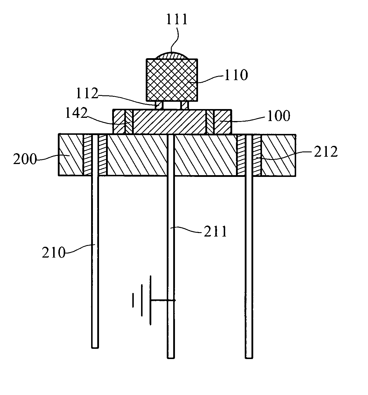
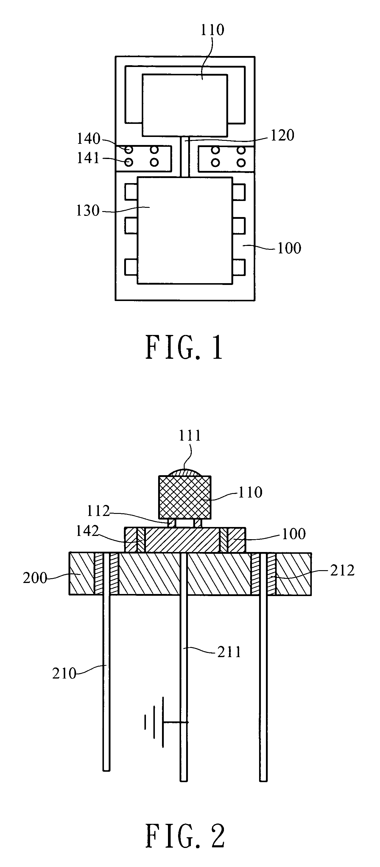
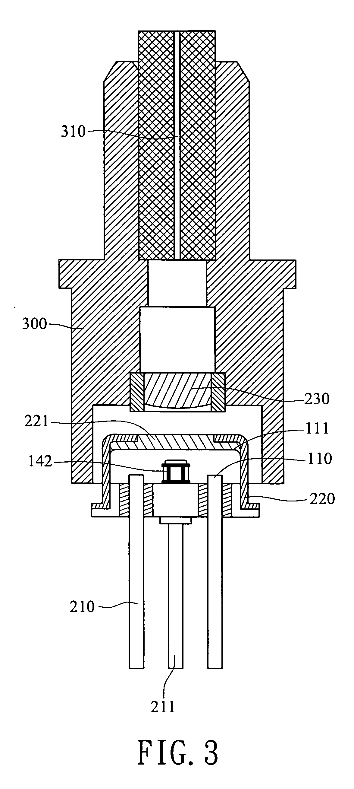
[0016] In the invention, the anode and cathode of the photoreceiver are coplanar (i.e. back-received photodidoe) and connected to the traces so as to reduce the parasitic impedance effect, improve the high speed performance of the optical subassembly and reduce the package size.

[0017] As shown in FIG. 1, a constructional view of a photodiode and a transimpedance amplifier in an embodiment of the invention, the photodiode 110 and the transimpedance amplifier 130 are electrically connected to the high-speed traces 120 formed on surface of the ceramic substrate 100. The positive and negative pins of the photodiode 110 are coplanar and connected to the high-speed traces 120. The transimpedance amplifier 130 is electrically connected to the high-speed traces 120 via flip chip, wire bonding or other methods. The high-speed traces 120 connected between the photodiode 110 and the transimpedance amplifier 130 surround with the ground pads 140. The ground pads 140 also electrically connect d...


PUM


Abstract

A receiver optical subassembly for transforming received optical signal into electrical signal includes at least a ceramic substrate, a photo receiver and a transimpedance amplifier. There are high-speed traces formed on the substrate. The positive and negative pads of the photo receiver are coplanar and connected to the traces without wire bonding so as to reduce the parasitic impedance effect and improve the high-speed performance of the optical subassembly. The transimpedance amplifier is electrically connected to the traces via flip chip, wire bonding or other methods. The photo receiver and the transimpedance amplifier are connected via the high-speed traces formed on the substrate.

Description

BACKGROUND OF THE INVENTION [0001] 1. Field of the Invention [0002] The invention generally relates to an optical transmission module, and in particular relates to a receiver optical subassembly. [0003] 2. Related Art [0004] In the trend of high transmission-rate communication, optical data transmission is being fast developed, and the related fiber optic products are getting more and more important. An optical data transmission system applying optical fiber media requires high transmission rate, low noise and of precise alignment of high quality optical transmission modules in order to meet user's needs. The key technologies for optical transmission modules are high-speed components, optical subassembly, alignment package and so on. [0005] Currently, the optical transceivers are mainly of surface emitting and surface receiving elements, such as vertical cavity surface emitting lasers (VCSEL). The package of the optical transceiver has to provide good alignment of the transceiver an...

Claims


Application Information

Patent Timeline
Patent Type & Authority Applications(United States)
IPC IPC(8): H01L29/267H01L33/00
CPCG02B6/4206H01L31/0232H01L31/0203G02B6/423H01L31/02327
Inventor WANG, CHIUNG-HUNLEE, CHUN-HSINGCHEN, YI-MINGLEE, SHIN-GECHEN, CHIH-LIHUANG, MING-FAHSU, CHIH-HAO
Owner IND TECH RES INST
Why Eureka
Try Eureka