Process for making circuit board or lead frame

a technology of lead frame and circuit board, which is applied in the direction of printed circuit manufacturing, lithography/patterning, patterning and lithography, etc., can solve the problems of difficult to secure a sufficient width and difficult to achieve a fine structur

Inactive Publication Date: 2005-06-09
SHINKO ELECTRIC IND CO LTD
View PDF4 Cites 42 Cited by
  • Summary
  • Abstract
  • Description
  • Claims
  • Application Information

AI Technical Summary

Benefits of technology

[0009] Accordingly, it is an object of this invention to provide a method of fabricating a circuit board or a lead frame with a fine conductor pattern by use of an inexpensive, simple subtractive method or a patterning technique and an etching technique, and a circuit board or a lead frame fabricated by the method.

Problems solved by technology

With the recent trend toward a higher integration and a finer structure of semiconductor devices and various electronic appliances, however, this method is disadvantageous when producing a fine conductor pattern for the circuit board.
An attempt to reduce the width of each pattern portion 5 or the pitch (c) between adjacent pattern portions would make it difficult to secure a sufficient width especially at the upper part of the pattern 5 far from the resin substrate 1, which in turn makes it difficult to achieve a fine structure.

Method used


Image

  • Process for making circuit board or lead frame
  • Process for making circuit board or lead frame
  • Process for making circuit board or lead frame

Examples


first embodiment

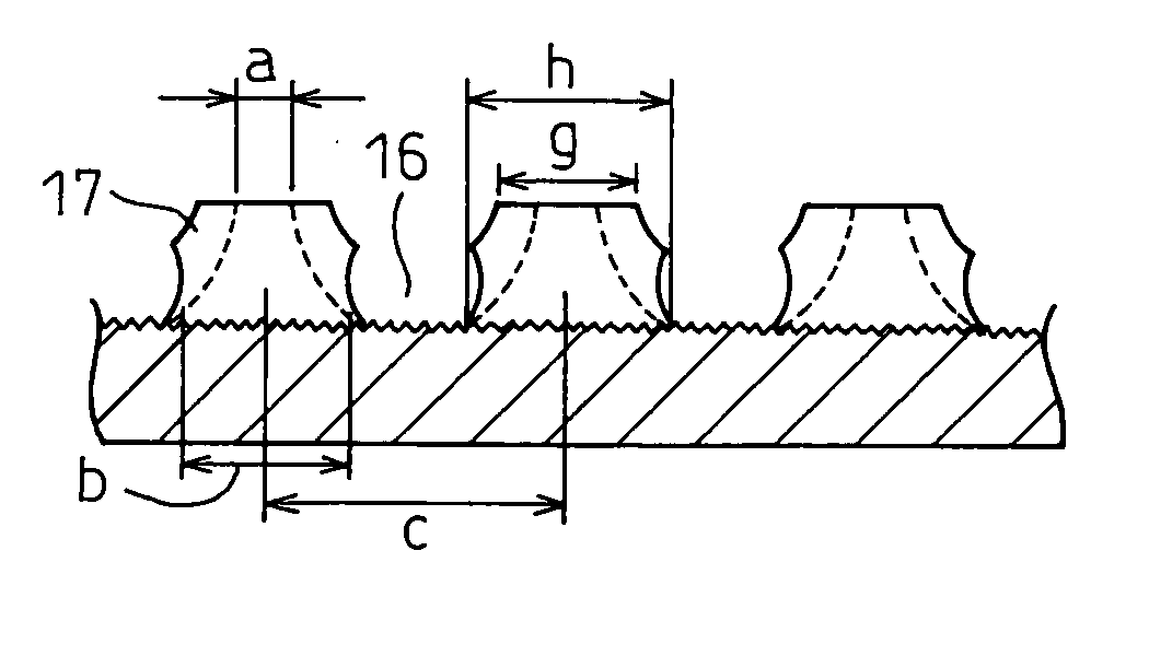
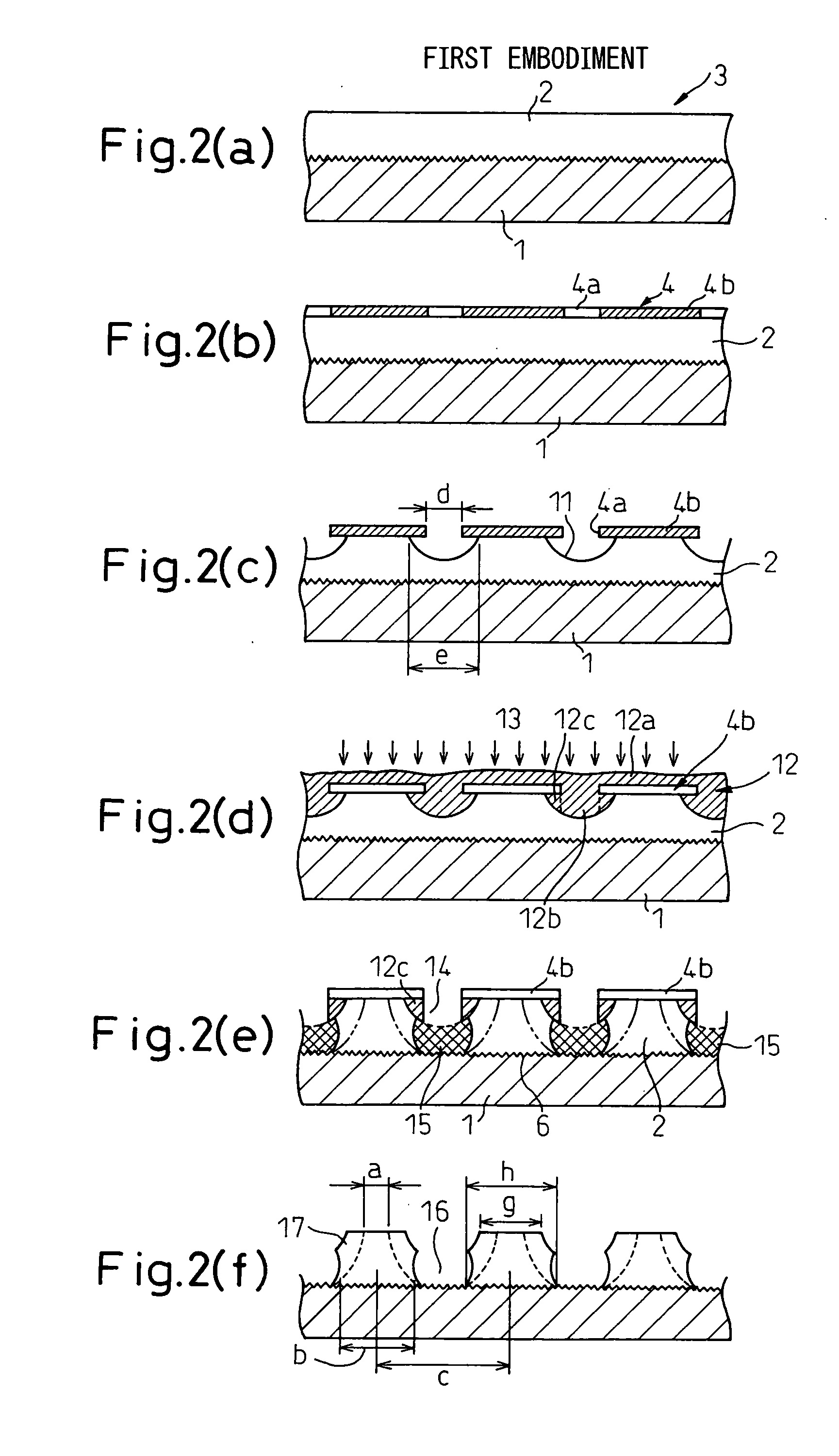
[0038] FIGS. 2(a) to 2(f) are sectional views showing the process of fabricating a circuit board using the subtractive method according to the invention.

[0039] In FIG. 2(a), a copper foil 2 is formed as a metal layer on a resin substrate 1 by a well-known method thereby to make up a substrate member 3. The resin substrate 1 is generally constituted of epoxy resin or glass epoxy resin.

[0040] Next, in FIG. 2(b), a dry film resist (DFR) having a light-blocking characteristic is formed as a first masking 4 on the upper surface of the copper foil 2, and exposed and developed by a well-known method thereby to form a resist pattern 4b.

[0041] Next, in FIG. 2(c), the etching solution is applied toward the first masking 4 formed of the openings 4a and the resist pattern 4b thereby to conduct the half etching. This half etching melts the peripheral area of the copper foil 2 under the etching solution passed portions 4a of the first masking 4. Thus, the half etching conditions (etching time, ...

second embodiment

[0051] First, as shown in FIG. 3(a), a thin second metal layer 20 is formed on the copper foil 2 of a substrate member 3 including a resin substrate 1 formed with a copper foil 2 constituting a first metal layer. The thin second metal layer 20 may be a silver plating as described later.

[0052] Next, as shown in FIG. 3(b), as in the first embodiment, a dry film resist (DFR) is formed as a first resist 4 on the upper surface of the second metal layer 20, and exposed and developed by a well-known method thereby to form a resist pattern 4b.

[0053] In FIG. 3(c), only the thin second metal layer 20 is selectively removed by the quick etching process through each opening 4a of the patterned first resist 4 formed on the upper surface of the second metal layer 20. As a result, only the portion of the second metal layer 20 corresponding to each opening 4a of the first resist 4 is removed. In the case where silver is used for the second metal layer 20, for example, the parting solution as desc...

fourth embodiment

[0085] FIGS. 9(a) to 9(f) are sectional views showing the fabrication process of a circuit board according to the invention using the subtractive method.

[0086]FIG. 9(a) shows a state in which a copper foil 102 is formed on a resin substrate 101 by a well-known method to make up a substrate member 103. The resin substrate 101 is generally formed of epoxy resin or glass-epoxy resin.

[0087] Next, in FIG. 9(b), a dry film resist (DFR) is formed as a first masking 104 on the upper surface of the copper foil, and exposed and developed by a well-known method thereby to form a resist pattern 104b.

[0088] Next, in FIG. 9(c), the etching solution is applied toward the first masking 104 of the resist pattern thereby to conduct the half etching. This half etching melts the peripheral area of the copper foil 102 under the etching solution passed portion 104a of the first masking 104. The half etching conditions (etching time, etc.) are adjusted so that the etched portion 111 of the copper foil 1...


PUM


Abstract

A process for forming a metal pattern comprising the following steps of: (a) half-etching a metal plate from one or respective sides thereof by means of first masking which is positioned on one or respective surfaces of the metal plate; (b) applying positive liquid resist on the half-etched metal plate from one or respective sides of the first masking; (c) exposing the positive liquid resist with light from one or respective sides of the first masking; (d) developing the positive liquid resist in such a manner that unexposed positive liquid resist located under the first masking is protected and exposed, uncured liquid resist is removed; (e) half-etching again the metal plate from one or respective sides thereof by means of second masking composed of the first masking and the protected positive liquid resist; (f) repeating the steps (b) to (e) until a metal pattern is obtained from the metal plate; and (g) removing the first masking, and the second or subsequent masking of the unexposed positive liquid resist, from the metal plate.

Description

CROSS-REFERENCE TO RELATED APPLICATIONS [0001] This application is a continuation-in-part (CIP) application of U.S. patent application Ser. No. 10 / 822,825 filed on Apr. 13, 2004, the contents being incorporated therein by reference.BACKGROUND OF THE INVENTION [0002] 1. Field of the Invention [0003] The present invention relates to a process for making a circuit board or a lead frame. In particular, the present invention relates to a process for making a circuit board with a conductor pattern formed on an insulating substrate by the subtractive method, or a process for making a lead frame or a fine pattern from a metal plate using a patterning technique. [0004] 2. Description of the Related Art [0005] The subtractive method is an inexpensive, simple method and has conventionally been used most widely for fabricating circuit boards. With the recent trend toward a higher integration and a finer structure of semiconductor devices and various electronic appliances, however, this method i...

Claims


Application Information

Patent Timeline
Patent Type & Authority Applications(United States)
IPC IPC(8): H01L21/48H05K3/06H05K3/20
CPCH01L21/4821H01L21/4828H01L21/4846H05K3/062H05K3/064H05K2203/1476H05K2203/0369H05K2203/0508H05K2203/058H05K2203/0597H05K3/202
Inventor FUKASE, KATSUYASAKAI, TOYOAKI
Owner SHINKO ELECTRIC IND CO LTD
Why Eureka
Try Eureka