Semiconductor integrated device

a technology of integrated devices and semiconductors, applied in the direction of pulse automatic control, pulse generation/distributing signals, pulse techniques, etc., can solve problems such as affecting the characteristics of the pll loop, and achieve the effects of reducing the amount of current, improving the jitter characteristics of high-speed clock signals, and reducing costs

Active Publication Date: 2005-06-16
SEIKO EPSON CORP
View PDF2 Cites 4 Cited by
  • Summary
  • Abstract
  • Description
  • Claims
  • Application Information

AI Technical Summary

Benefits of technology

[0027] With the present invention composed as such, it is possible to significantly reduce the amount of current that is excessively consumed for generating high-speed clock signals that are necessary for signal processing.
[0028] Furthermore, with the present invention, it is possible to significantly improve the jitter characteristics of the high-speed clock signals that are necessary for signal processing upon generating these high-speed clock signals, and to prevent malfunctions upon conducting signal processing with these clock signals.
[0029] Further, with the present invention, it is possible to eliminate the need for an external capacitor, thereby cutting costs by reducing the number of unit items, and preventing its characteristics from worsening because of the use of such an external capacitor.

Problems solved by technology

Moreover, in conventional semiconductor integrated devices, a capacitor used for a loop filter composing a PLL circuit is provided externally as described above, thus impairing the characteristics of the PLL loop.

Method used


Image

  • Semiconductor integrated device
  • Semiconductor integrated device
  • Semiconductor integrated device

Examples


Embodiment Construction

[0036] An embodiment of this invention will now be described with references to the accompanying drawings.

[0037] Prior to the description of the embodiment of the present invention, the basic principles of this invention are described.

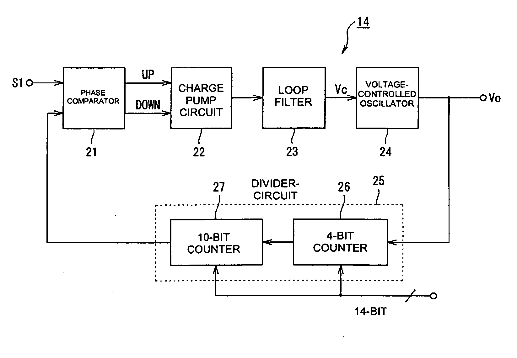
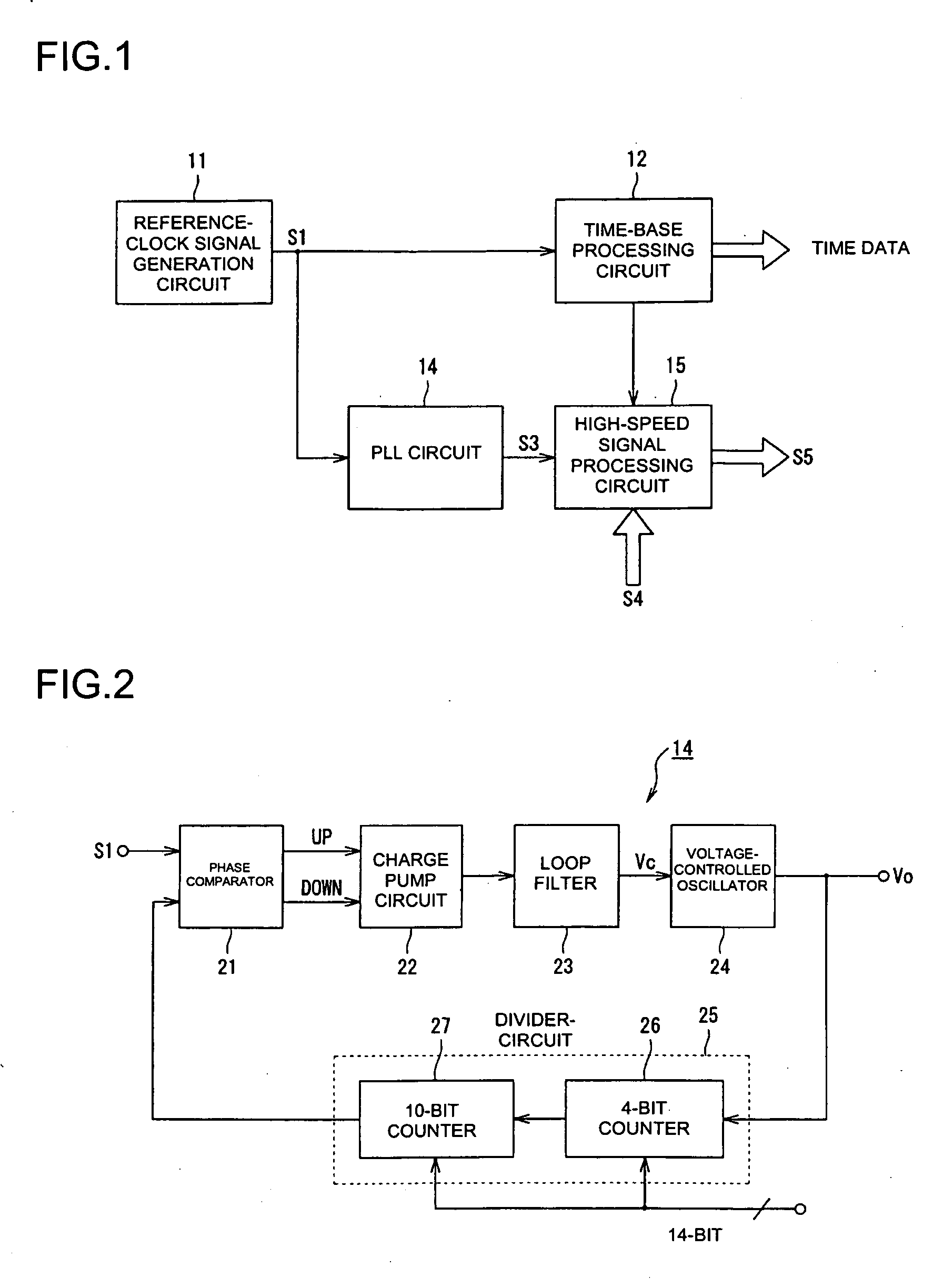
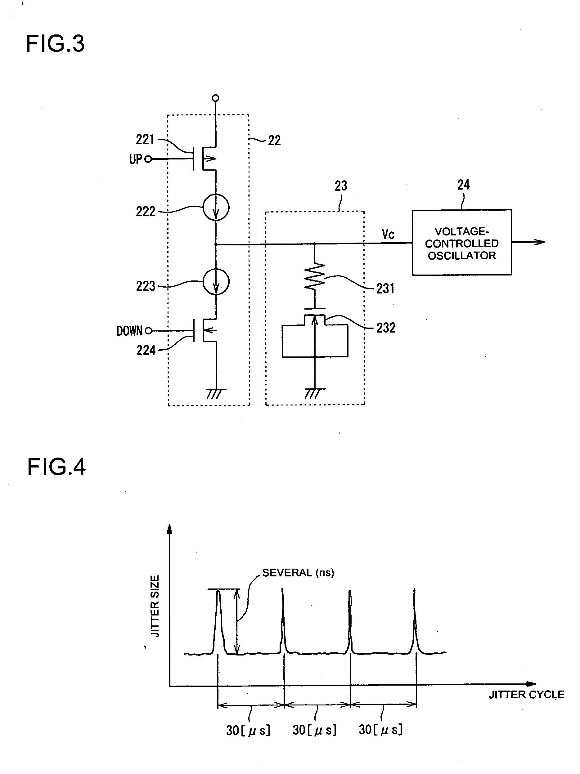
[0038] The present invention uses a low-speed base-clock signal for time base to generate high-speed clock signals that are necessary for signal processing, and prevents excessive current consumption. For this reason, as FIG. 1 shows, a base-clock signal S1 generated by a base-clock signal generation circuit 11 is provided to a time-base processing circuit 12 and to a PLL circuit 14 individually.

[0039] The present invention also makes it possible to generate a high-speed clock signal S3, while setting the range of the base-clock signal S1, generated by the base-clock signal generation circuit 11, low, for example, from 10 kHz to 100 kHz, and setting a factor N by which the PLL circuit 14 multiplies the base-clock signal S1 high, such as at least 100...


PUM


Abstract

A structure is provided for significantly reducing the current excessively consumed for generating a high-speed clock signal necessary for signal processing, and significantly improve the jitter characteristics of the high-speed clock signal. The structure includes a reference-clock signal generation circuit, a time-base processing circuit, a PLL circuit, and a high-speed signal processing circuit. A low-speed reference-clock signal generated by the reference-clock signal generation circuit is provided to the PLL circuit. The PLL circuit generates a high-speed clock signal by multiplying the reference-clock signal by a factor of N. The factor N is at least 100. To reduce a jitter of the high-speed clock signal generated by the PLL circuit, a natural angular frequency ωn and a damping factor ζ that relate to the response characteristics of the system of the PLL circuit are set to range from 3 kHz to 10 kHz, and 0.01 or less, respectively.

Description

RELATED APPLICATIONS [0001] This application claims priority to Japanese Patent Application No. 2003-400027 filed Nov. 28, 2003 which is hereby expressly incorporated by reference herein in its entirety. BACKGROUND [0002] 1. Field of the Invention [0003] The present invention relates to a semiconductor integrated device equipped with a reference-clock signal generation circuit that generates a low-speed reference-clock signal, and a high-speed signal processing circuit that can conduct high-speed signal processing. [0004] 2. Related Art [0005] A conventional semiconductor integrated device is equipped with, as shown in FIG. 6, a reference-clock signal generation circuit 1, a time-base processing circuit 2, a fundamental-frequency-oscillation circuit 3, a phase-locked loop (PLL) circuit 4, and a high-speed signal processing circuit 5. [0006] In a semiconductor integrated device composed as illustrated, the reference-clock signal generation circuit 1 is constituted of a quartz-oscilla...

Claims


Application Information

Patent Timeline
Patent Type & Authority Applications(United States)
IPC IPC(8): G06F1/10H03K5/00H03L7/06H03L7/093H03L7/099H03L7/18
CPCH03L7/18H03L7/0996
Inventor FURUYA, YASUNARI
Owner SEIKO EPSON CORP
Why Eureka
Try Eureka