Redundant single event upset supression system

a supression system and single event technology, applied in the field of integrated circuit design, can solve the problem that the type of latches available to the designer no longer limits the design

Active Publication Date: 2005-06-16
FERMI RESEARCH ALLIANCE LLC
View PDF13 Cites 54 Cited by
  • Summary
  • Abstract
  • Description
  • Claims
  • Application Information

AI Technical Summary

Benefits of technology

[0024] It is another feature of this present invention that it is logically flexible. Where the present invention is configured as an SEU tolerant SR flip-flop, it can be converted into any known type of latch (e.g. SR latch, D-latch, clocked D-latch, T-flip-flops, JK flip-flops, etc.) by simple applications of external logic and without altering the internal architecture. This has two benefits. First, the type of latch available to the designer no longer limits designs. Second, the SEU tolerance of the register is not affected by the addition of external logic. The SR latch has essentially the same SEU tolerance as the clocked D-latch and the JK flip-flop.
[0027] It is yet another feature of the present invention that, from the perspective of a designer, it is reliable and predictable. When overdriving is required, process variations can render a design non-functional. In the present invention, however, changing the inputs is guaranteed to change the outputs because all inputs are gates and overdriving is not required. The change of output is only a matter of time relative to the change of input. The time required to do this is well and reliably predicted by modern Computer-Aided Design (CAD) software. Therefore, the performance of the present invention can always be reliably predicted before a company spends the money to fabricate a design.
[0030] It is a feature of this present invention that, because asynchronous sets and resets are possible, external, and redundant circuitry with auto-correction can be easily added to this present invention to increase its SEU tolerance even further.

Problems solved by technology

First, the type of latch available to the designer no longer limits designs.

Method used


Image

  • Redundant single event upset supression system
  • Redundant single event upset supression system
  • Redundant single event upset supression system

Examples


Embodiment Construction

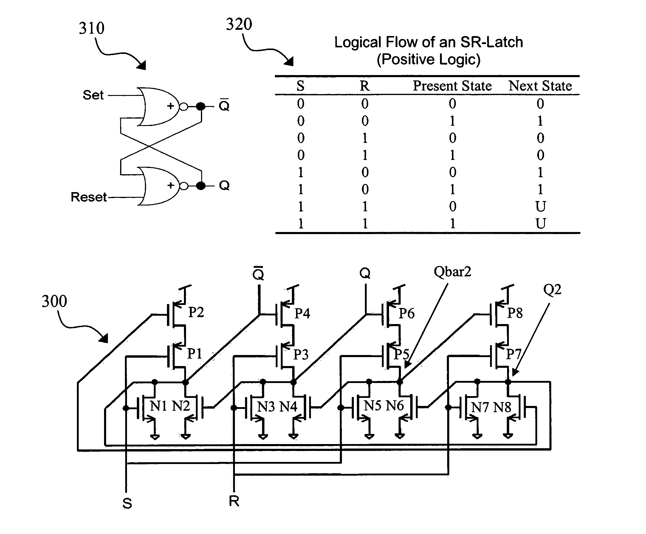
[0048] A schematic diagram for a single event upset tolerant positive logic SR flip-flop 300 is shown in FIG. 3 along with the canonical schematic 310 it emulates and a table 320 of the logic it performs. Since this SEUSS Cell emulates a cross-coupled Nor Gate SR flip-flop, it is called a SEUSSNor. According to the schematic, a cell can be provided having inputs S and R. Inputs S and R only drive the gates of transistors (N1, P1), (N3, P3), (N5, P5), and (N7, P7).

[0049] External circuitry driving the cell cannot possibly experience any “back drive” (i.e., no current is driven back out the inputs by the SEUSSNor towards the external circuitry) because CMOS gates are insulators. Moreover, regardless of how weak the external circuitry is and regardless of how strong the SEUSSNor's internal circuitry is made, the next state is the inevitable result of the inputs only. Stronger internal circuitry simply increases the input capacitance of the SEUSSNor. Weaker external circuitry simply in...


PUM


Abstract

CMOS transistors are configured to operate as either a redundant, SEU-tolerant, positive-logic, cross-coupled Nor Gate SR-flip flop or a redundant, SEU-tolerant, negative-logic, cross-coupled Nand Gate SR-flip flop. The register can operate as a memory, and further as a memory that can overcome the effects of radiation. As an SR-flip flop, the invention can be altered into any known type of latch or flip-flop by the application of external logic, thereby extending radiation tolerance to devices previously incapable of radiation tolerance. Numerous registers can be logically connected and replicated thereby being electronically configured to operate as a redundant circuit.

Description

GOVERNMENT INTEREST [0001] The United States Federal Government has right to this invention pursuant to Contract No. DE-AC02-76CH03000 between Universities Research Corporation and the United States Department of Energy.FIELD OF THE INVENTION [0002] The present invention is generally related to integrated circuit design. More particularly, the present invention is related to methods and systems preventing single event upset in integrated circuits and memory cells. Additionally, the present invention is related to methods and systems preventing upset in integrated circuits and memory cells by utilizing a design of redundant single event upset tolerant registers. BACKGROUND [0003] The effects of radiation on integrated circuits have been known for over thirty years. These effects can be broken down into two broad categories. The first category is “total dose effects” in which an integrated circuit gradually deteriorates due to the accumulated effect of all the damage done to the cryst...

Claims


Application Information

Patent Timeline
Patent Type & Authority Applications(United States)
IPC IPC(8): G11C11/412H03K3/037H03K19/003
CPCG11C11/4125H03K19/00392H03K19/00338H03K3/0375
Inventor HOFF, JAMES R.
Owner FERMI RESEARCH ALLIANCE LLC
Why Eureka
Try Eureka