Device and method for image sensing

a technology of image sensing and image sensor, applied in the field of image sensing, can solve the problems of significant noise source, noise associated with conventional cmos image sensing devices, and drawbacks of particular applications and users

Inactive Publication Date: 2005-06-16
RE SECURED NETWORKS LLC +1
View PDF30 Cites 132 Cited by
  • Summary
  • Abstract
  • Description
  • Claims
  • Application Information

AI Technical Summary

Benefits of technology

[0011] In yet another aspect, the invention features a CMOS image sensor circuit including a plurality of photodiodes, each of the plurality of photodiodes associated with a pixel of an imaging array, the pixel having a pitch of about 3 microns or less, and a plurality of transfer transistors, each of the plurality of transfer transistors connecting a corresponding one of the plurality of photodiodes to a shared sense node, the shared sense node configured to store a charge collected by each of the plurality of photodiodes. This aspect further includes a shared readout circuit including a reset transistor, a source follower transistor, and a select transistor, the reset transistor being connected to the shared sense node and configured to reset the shared sense node. In this...

Problems solved by technology

However, such conventional CMOS image sensing devices may have drawbacks for particular applications and users.
For example, some conventional CMOS image sensing devices suffer from noise associated with the process for resetting each photodiode to a known potential after each exposure and in preparation for the next image.
This noise, which is associated with the gate capacitor of a field effect transistor (“FET”), has been referred to as “reset noise” or “KTC noise,” and can be a significant source of noise in camera systems that employ conventional CMOS image sensing technology.
Reducing the capacitance of the sensing node may reduce reset noise in some devices, but it may also cause a corresponding reduction in the total charge that can be collected—ther...

Method used


Image

  • Device and method for image sensing
  • Device and method for image sensing
  • Device and method for image sensing

Examples


Embodiment Construction

[0022] Various embodiments of devices, systems, and methods in accordance with the present invention will now be described with reference to the drawings.

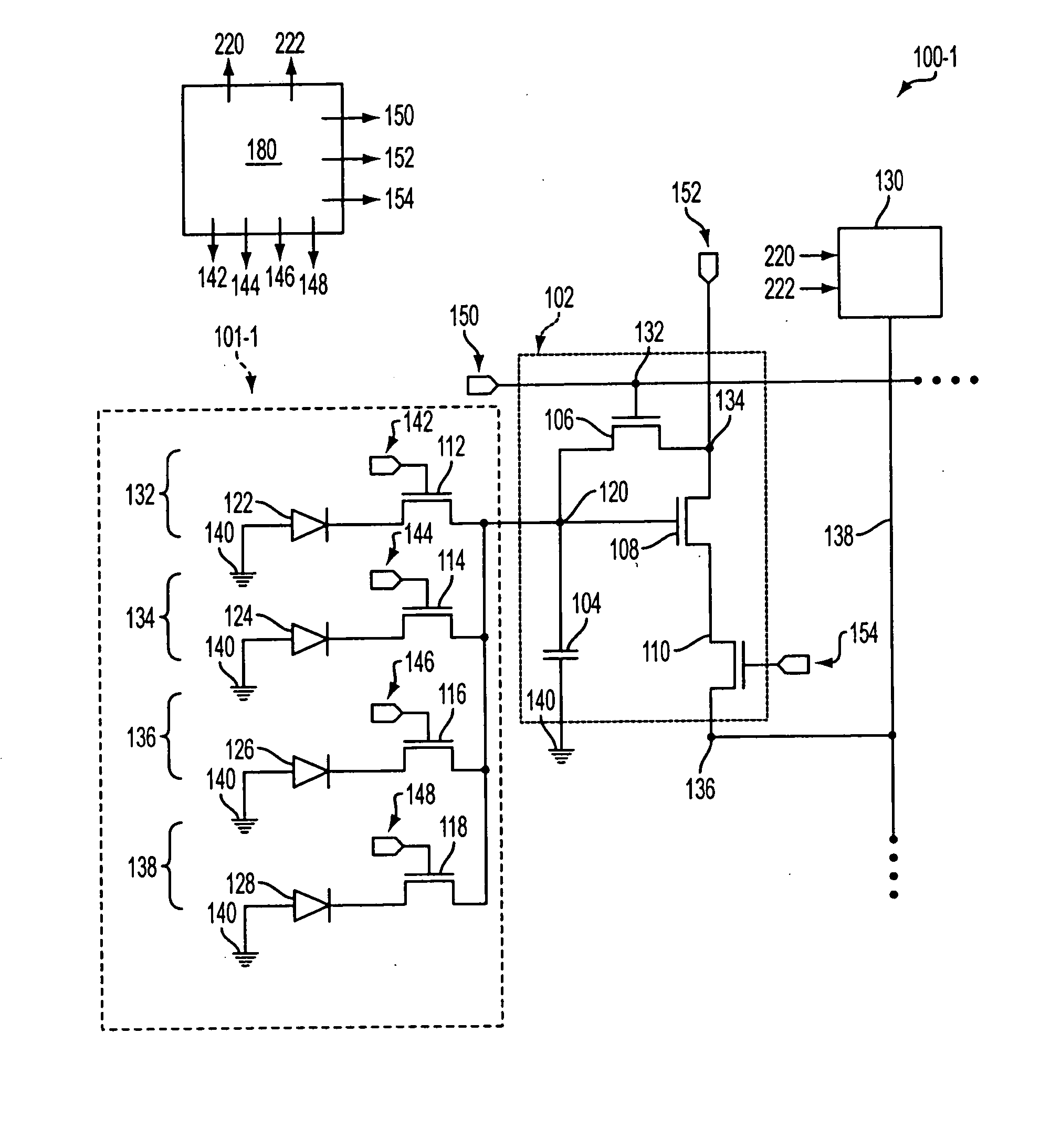
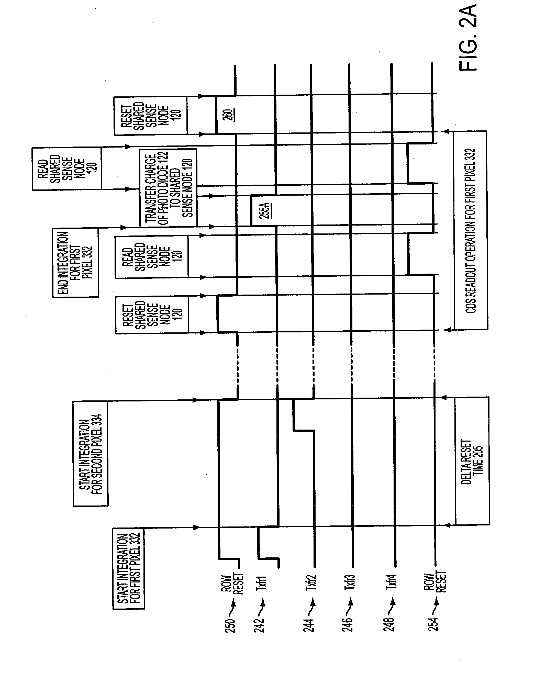
[0023]FIG. 1 shows a schematic diagram of an image sensor circuit 100-1 according to one embodiment of the invention. This embodiment of the image sensor circuit 100-1 includes a shared readout circuit 102 that generally includes a shared sense node 120, a reset device 106, a source follower device 108, and a select device 110. The image sensor circuit 100-1 of one embodiment may be used in a variety of applications including imaging devices such as a digital camera 60 or a mobile phone 70. One embodiment of an image sensor circuit 100-1 may be configured to control and read a plurality of pixels 132, 134, 136, 138, each of which is a single addressable point that produces picture information. In this embodiment, each pixel 132, 134, 136, 138 includes a photodetector 122, 124, 126, 128 and a transfer device 142, 144, 146, 148. In ...


PUM


Abstract

The present invention relates to devices and methods for image sensing. In one aspect, the present invention relates to a device including a plurality of pixels, wherein each pixel includes a charge transfer device and photodetector, and each of the pixels has a pitch of about 3 microns or less. This aspect further includes a select transistor, a reset transistor, a source follower transistor, and a sense node, wherein the select transistor, the reset transistor, the source follower transistor, and the sense node are shared by the plurality of pixels.

Description

FIELD OF THE INVENTION [0001] The present invention generally relates to imaging technology and, more particularly, to solid state devices and methods for sensing images using a number of pixels. BACKGROUND OF THE INVENTION [0002] Certain conventional image sensing devices have been used to convert an image into a signal indicative of the image. Conventional image sensing technology includes certain charge coupled devices (“CCD”), certain complimentary metal oxide semiconductors (“CMOS”), and other devices. [0003] In recent years, for certain applications and users, CMOS image sensing devices have become practical and provide cost and power advantages over other technologies, such as CCD. Conventional CMOS image sensing devices have been fabricated from semiconductor materials and include imaging arrays of light detecting (i.e., photosensitive) elements called “photodetectors.” Such photodetectors have been used to generate analog signals representative of a particular image present...

Claims


Application Information

Patent Timeline
IPC IPC(8): H01L27/00H01L27/146H04NH04N3/14H04N5/359H04N5/3745
CPCH01L27/14603H01L27/14643H01L27/14654H04N5/37457H04N5/3591H04N5/363H04N5/347H04N25/46H04N25/621H04N25/65H04N25/778
Inventor BENCUYA, SELIM S.LUO, JIAFUMANN, RICHARD A.
Owner RE SECURED NETWORKS LLC
Why Eureka
Try Eureka