Semiconductor device having two different operation modes employing an asymmetrical buried insulating layer and method for fabricating the same

a technology of asymmetric oxidation layer and asymmetric dram, which is applied in the direction of semiconductor devices, electrical appliances, transistors, etc., can solve the problems of short channel effect (sce), increase in leakage current, and deterioration of the refresh characteristic of dram devices, so as to improve the floating-body effect, increase the on-current, and reduce the off-current

Active Publication Date: 2005-06-23
SAMSUNG ELECTRONICS CO LTD
View PDF6 Cites 57 Cited by
  • Summary
  • Abstract
  • Description
  • Claims
  • Application Information

AI Technical Summary

Benefits of technology

[0011] Some embodiments of the invention provide a semiconductor device capable of increasing the on-current and decreasing the off-current compared to the conventional art while improving the floating-body effect. Other embodiments of the invention provide a DRAM cell capable of preventing the leak current to enhance the refresh characteristic while improving the floating-body effect. Other embodiments of the invention provide a method for fabricating the semiconductor device and the DRAM cell described above.

Problems solved by technology

As a result, shortened channel lengths of the MOS transistors may cause short channel effect (SCE).
However, the increased channel ion concentration also causes a leakage current to increase.
Increased leakage current leads to deterioration of the refresh characteristic of the DRAM device.
In addition, the transistor is electrically connected to the semiconductor substrate below the buried insulating layer to operate in a body-tied mode, which reduces the floating-body effect.

Method used


Image

  • Semiconductor device having two different operation modes employing an asymmetrical buried insulating layer and method for fabricating the same
  • Semiconductor device having two different operation modes employing an asymmetrical buried insulating layer and method for fabricating the same
  • Semiconductor device having two different operation modes employing an asymmetrical buried insulating layer and method for fabricating the same

Examples


Embodiment Construction

[0018] The invention will now be described more fully hereinafter with reference to the accompanying drawings, in which exemplary embodiments of the invention are shown. This invention may, however, be embodied in different forms and should not be construed as limited to the embodiments set forth herein. Rather, these embodiments are provided so that this disclosure will be thorough and complete, and will fully convey the scope of the invention to those skilled in the art. In the drawings, the thickness of layers and regions are exaggerated for clarity. Like numbers refer to like elements throughout the specification.

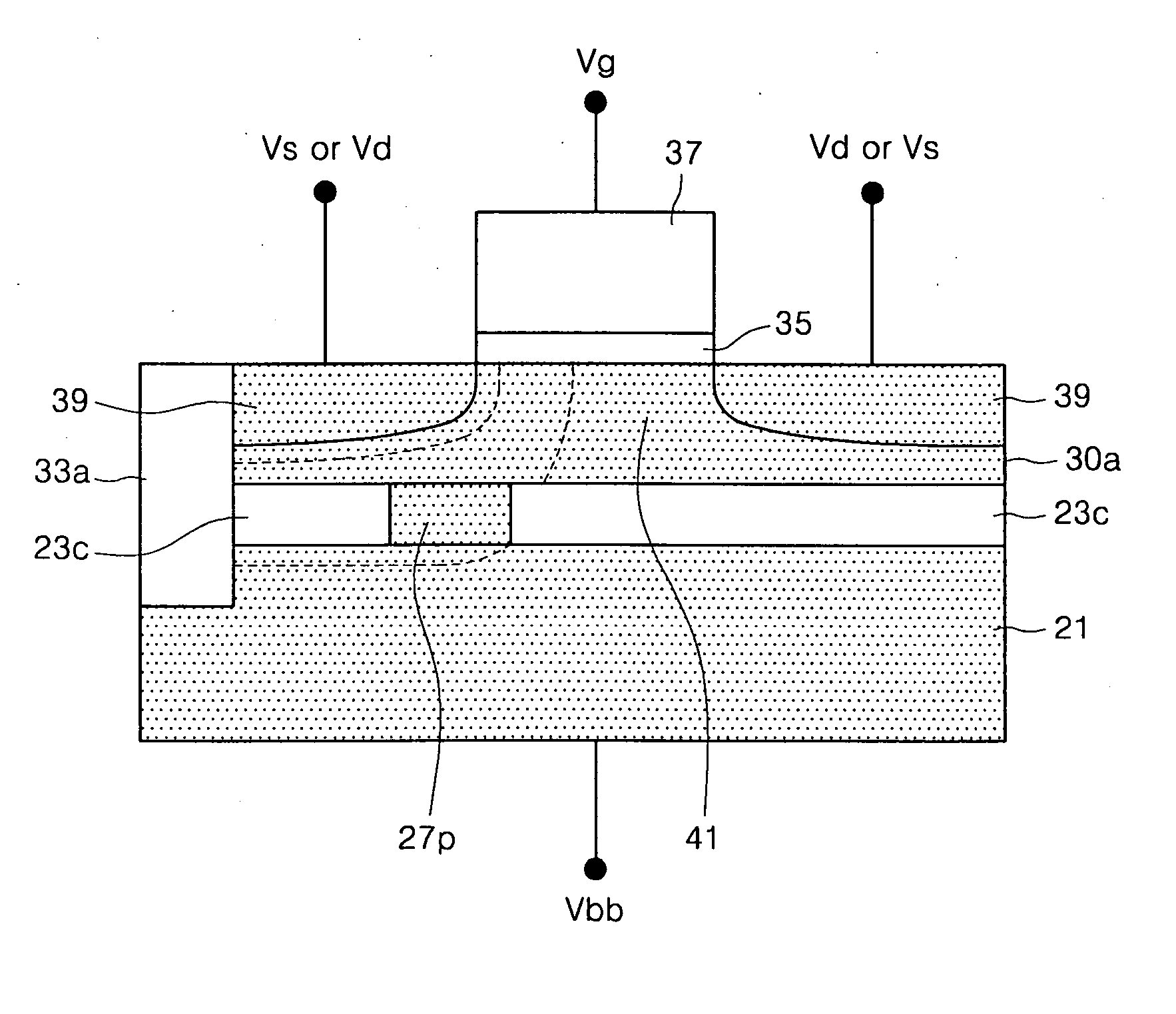
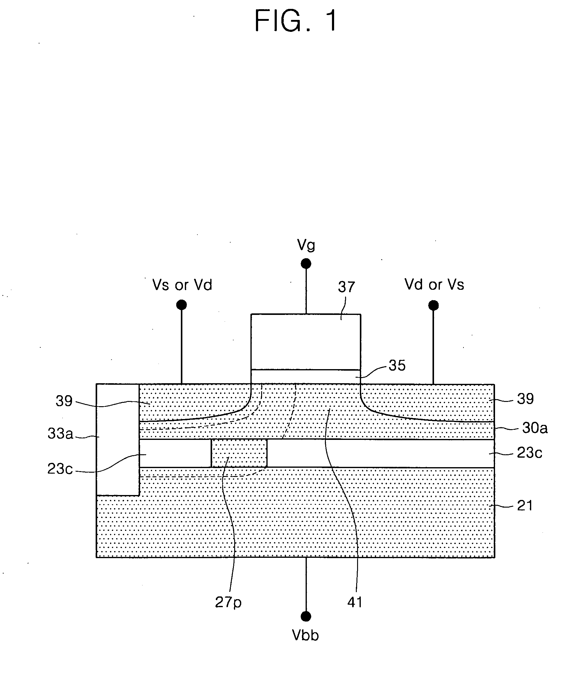
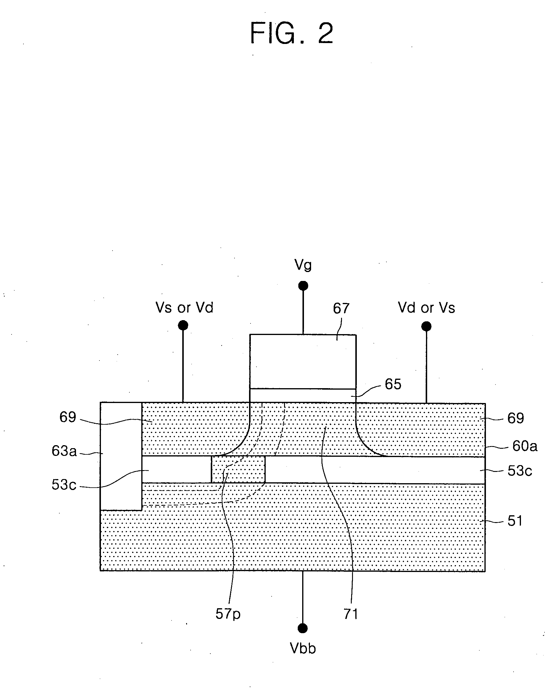
[0019]FIG. 1 and FIG. 2 are cross-sectional diagrams illustrating semiconductor devices having two different operation modes in accordance with some embodiments of the invention. FIG. 3 and FIG. 4 are cross-sectional diagrams illustrating a DRAM cell having two different operation modes in accordance with other embodiments of the invention.

[0020] Referring to FIG. 1, ...


PUM


Abstract

According to some embodiments, a semiconductor device includes a lower semiconductor substrate, an upper silicon pattern, and a MOS transistor. The MOS transistor includes a body region formed within the upper silicon pattern and source / drain regions separated by the body region. A buried insulating layer is interposed between the lower semiconductor substrate and the upper silicon pattern. A through plug penetrates the buried insulating layer and electrically connects the body region with the lower semiconductor substrate, the through plug positioned closer to one of the source / drain regions than the other source / drain region. At least some portion of the upper surface of the through plug is positioned outside a depletion layer when a source voltage is applied to the one of the source / drain regions, and the upper surface of the through plug is positioned inside the depletion layer when a drain voltage is applied to the one region.

Description

CROSS-REFERENCE TO RELATED APPLICATIONS [0001] This application claims priority from Korean Patent Application No. 2003-93975, filed on 19 Dec. 2003, the disclosure of which is hereby incorporated by reference in its entirety for all purposes. BACKGROUND OF THE INVENTION [0002] 1. Field of the Invention [0003] This disclosure relates to a semiconductor device and method for fabricating the same and, more particularly, to a semiconductor device having two different operation modes employing an asymmetrical buried oxidation layer and method for fabricating the same [0004] 2. Description of the Related Art [0005] Semiconductor devices employing a discrete device such as a metal oxide semiconductor (MOS) transistor as a switching device are widely used. Since the degree of integration of semiconductor devices is steadily increasing, the size of MOS transistors are correspondingly being scaled down. As a result, shortened channel lengths of the MOS transistors may cause short channel eff...

Claims


Application Information

Patent Timeline
Patent Type & Authority Applications(United States)
IPC IPC(8): H01L21/336H01L21/76H01L21/762H01L21/8242H01L27/02H01L27/108H01L29/76H01L29/78H01L29/786
CPCH01L27/0214H01L27/10802H01L29/78612H01L29/7841H01L27/10873H10B12/20H10B12/05H01L21/18
Inventor OH, CHANG-WOOPARK, DONG-GUNLEE, SUNG-YOUNGCHOE, JEONG-DONG
Owner SAMSUNG ELECTRONICS CO LTD
Why Eureka
Try Eureka