

Method of manufacturing semiconductor integrated circuit
a manufacturing method and integrated circuit technology, applied in semiconductor devices, semiconductor/solid-state device details, electrical devices, etc., can solve the problems of increasing the number of layers, significantly increasing the cost generated by increasing so as to reduce the number of required masks and reduce the cost of mask related costs. , the effect of reducing the cost of the total mask
- Summary
- Abstract
- Description
- Claims
- Application Information
AI Technical Summary
Benefits of technology
Problems solved by technology
Method used
Image

Examples
Embodiment Construction
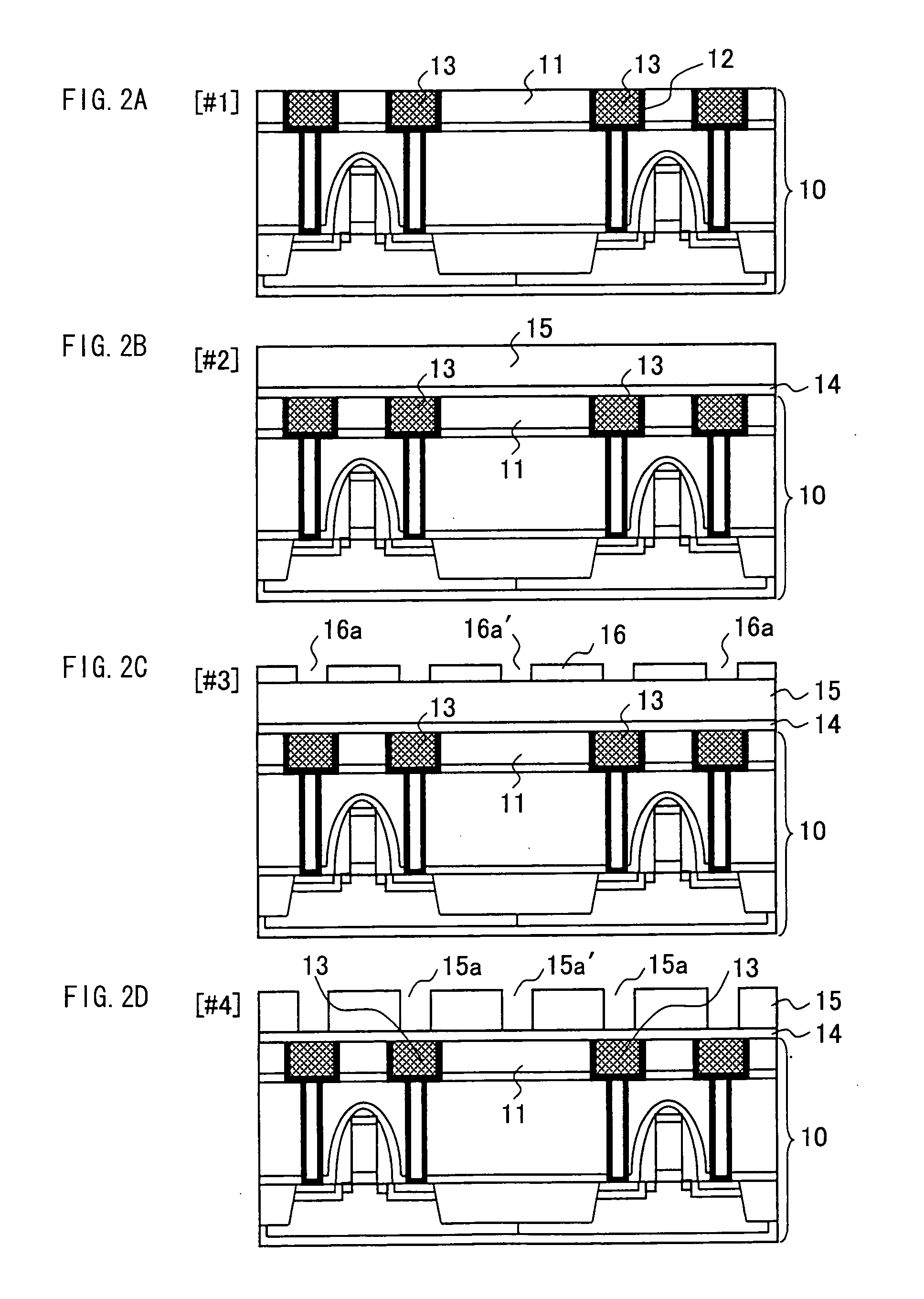
[0078] Hereinafter, a method of manufacturing a semiconductor integrated circuit according to a preferred embodiment of the present invention is described referring to the drawings.
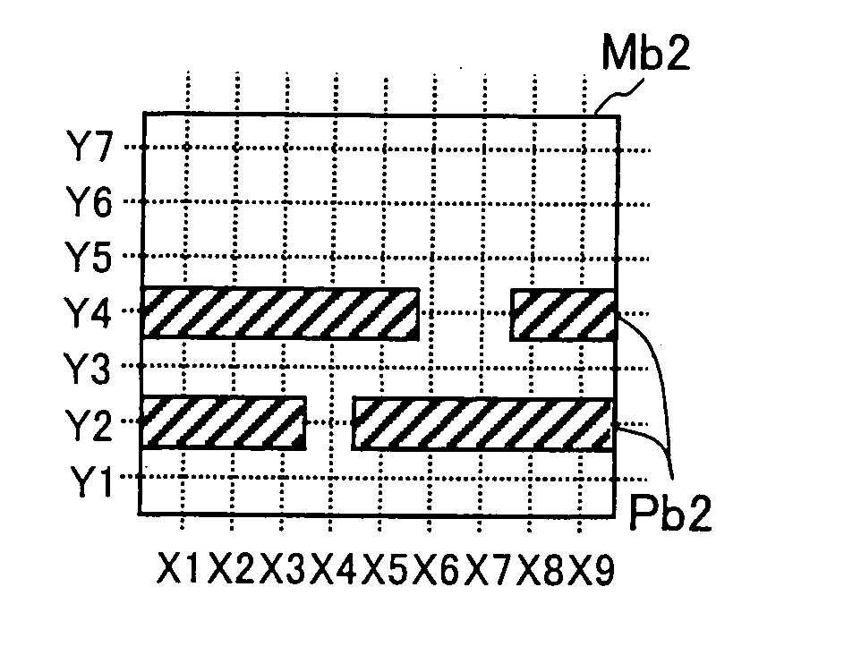
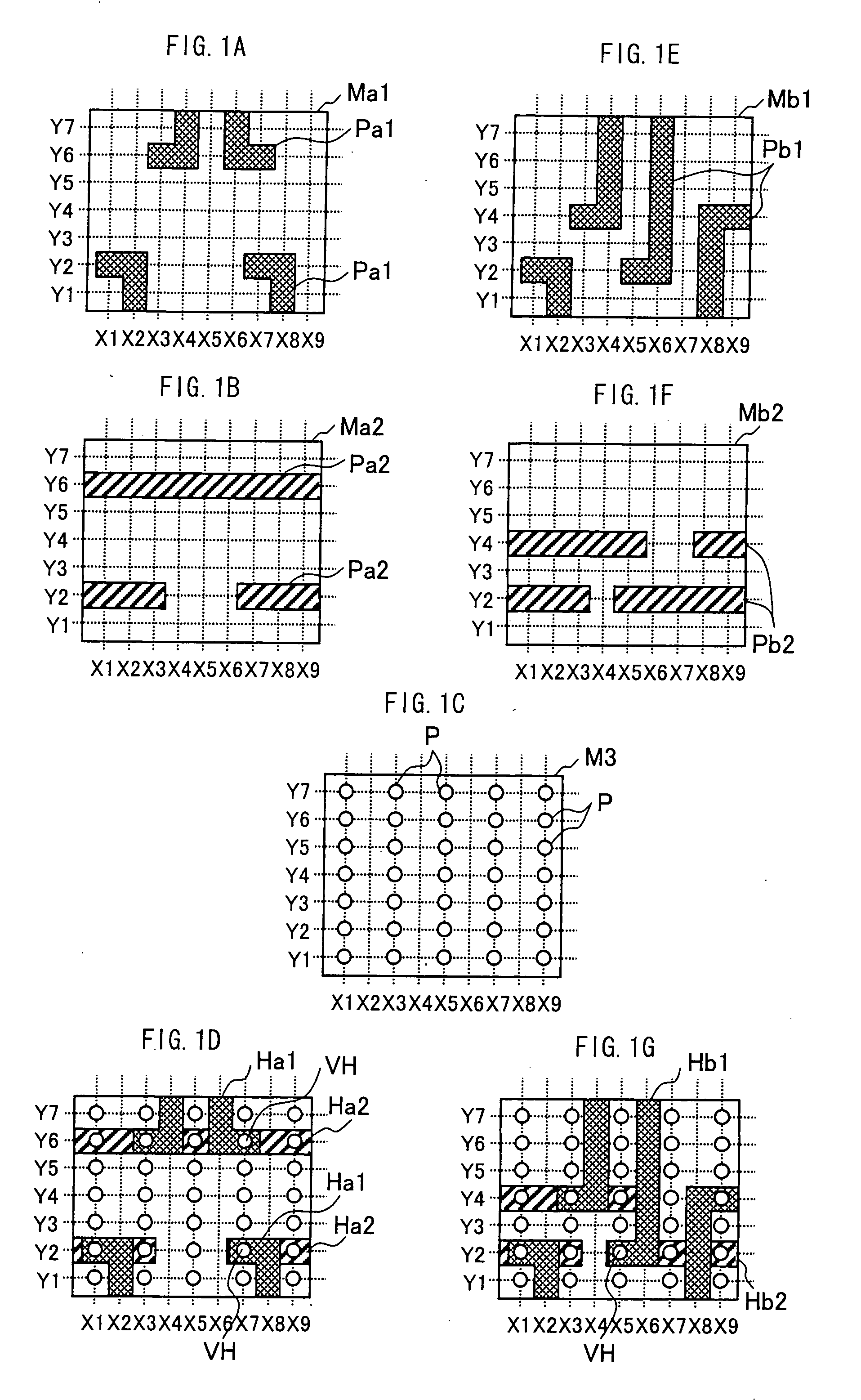
[0079] FIGS. 1A-G illustrate process flows used for describing the method of manufacturing the semiconductor integrated circuit according to the preferred embodiment. FIGS. 1A-1D are plan views used for describing a back-end part of a developed product A-a in a product class A of a semiconductor. FIGS. 1E-1G are plan views used for describing a back-end part of another developed product A-b in the same product class A of the semiconductor. FIGS. 1A-1G are sectioned therein by a plurality of vertical reference lines Xn (X1, X2, X3 . . . ) and a plurality of horizontal reference lines Yn (Y1, Y2, Y3 . . . ). FIG. 1C is common for the two process flows.
[0080]FIG. 1A illustrates a metal wiring mask Ma1 of an Nth layer of the developed product A-a.
[0081] In the metal wiring mask Ma1, a pattern Pa1 for a met...
PUM
 Abstract
Description
Claims
Application Information