Automated packaging apparatus and method of optical elements

a packaging apparatus and optical element technology, applied in the direction of soldering apparatus, manufacturing tools,auxillary welding devices, etc., can solve the problems of reducing the market scale of early applied soldering points, and reducing the cost of production. , to achieve the effect of effectively solving the conventional manual packaging process, reducing the time period required for performing the focusing operation, and reducing the cos

Inactive Publication Date: 2005-06-30
IND TECH RES INST
View PDF7 Cites 15 Cited by
  • Summary
  • Abstract
  • Description
  • Claims
  • Application Information

AI Technical Summary

Benefits of technology

[0008] An object of the invention is to provide an automatic packaging apparatus and an automatic packaging method of optical elements, which are capable of effectively solving the conventional manually packaging process. The time period required for performing the focusing operation can be shortened by using an automatic focusing platform. Furthermore, by means of an automatic solder-feeding unit, the solders are injected into a gap between components so as to minimize thermal strain. In such manner, the light loss resulted during the welding operation is reduced, and thus the performance of the components is enhanced. In addition, by controlling feeding amount of the solders and designing the components, the airtight requirement of the welding operation will be met, and thus the yield of the packaged components is increased and the artificial interference is avoided.

Problems solved by technology

The procedures associated with feeding, focusing, fixing and packaging operations are labor-intensive.
Due to this limitation, high fabricating cost, low production and low yield adversely affect mass production of such optical elements and thus the development of their market scale is restricted.
However, during a time period from the procedure of applying the soldering points to the procedure of melting the soldering points, since the manual process fails to meet the requirement of simultaneous processing operation, the early applied soldering points may be shrunk.
Therefore, the lower part has been focused may deviate from its original place such that the light loss is increased.
Since the packaging process is cumbersome and less reproducible, the uncertainty of packaging the components is increased.
Accordingly, the above-described prior art product is not a perfect design and has still many disadvantages to be solved.

Method used


Image

  • Automated packaging apparatus and method of optical elements
  • Automated packaging apparatus and method of optical elements
  • Automated packaging apparatus and method of optical elements

Examples


Embodiment Construction

[0018] The configuration, usage and feature of the present invention will become apparent from the detailed description to follow taken in conjunction with the preferred embodiments and drawings.

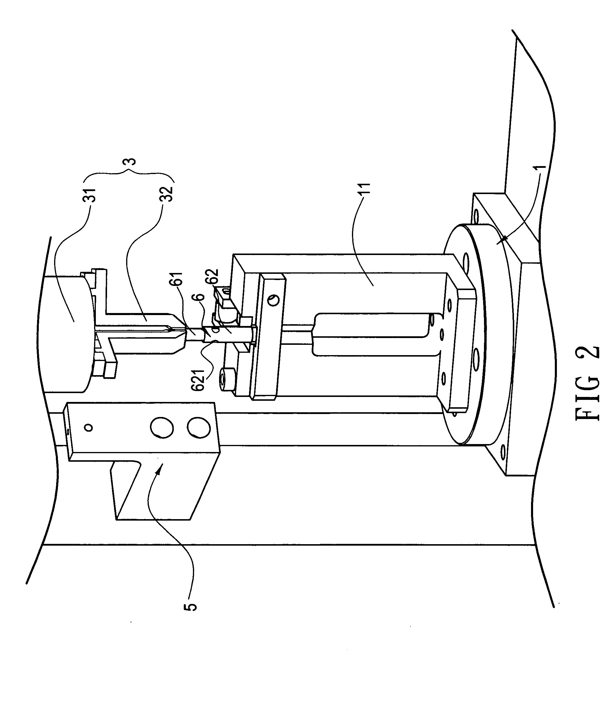
[0019] Referring to FIG. 3, the present invention is provided to package an upper part 61 and a lower part 62 of an optical element 6. Three solder feeding holes 521 are discretely arranged at regular intervals on a horizontal plane at the periphery of the lower part 62. The included angle between two adjacent holes 521 is 120°.

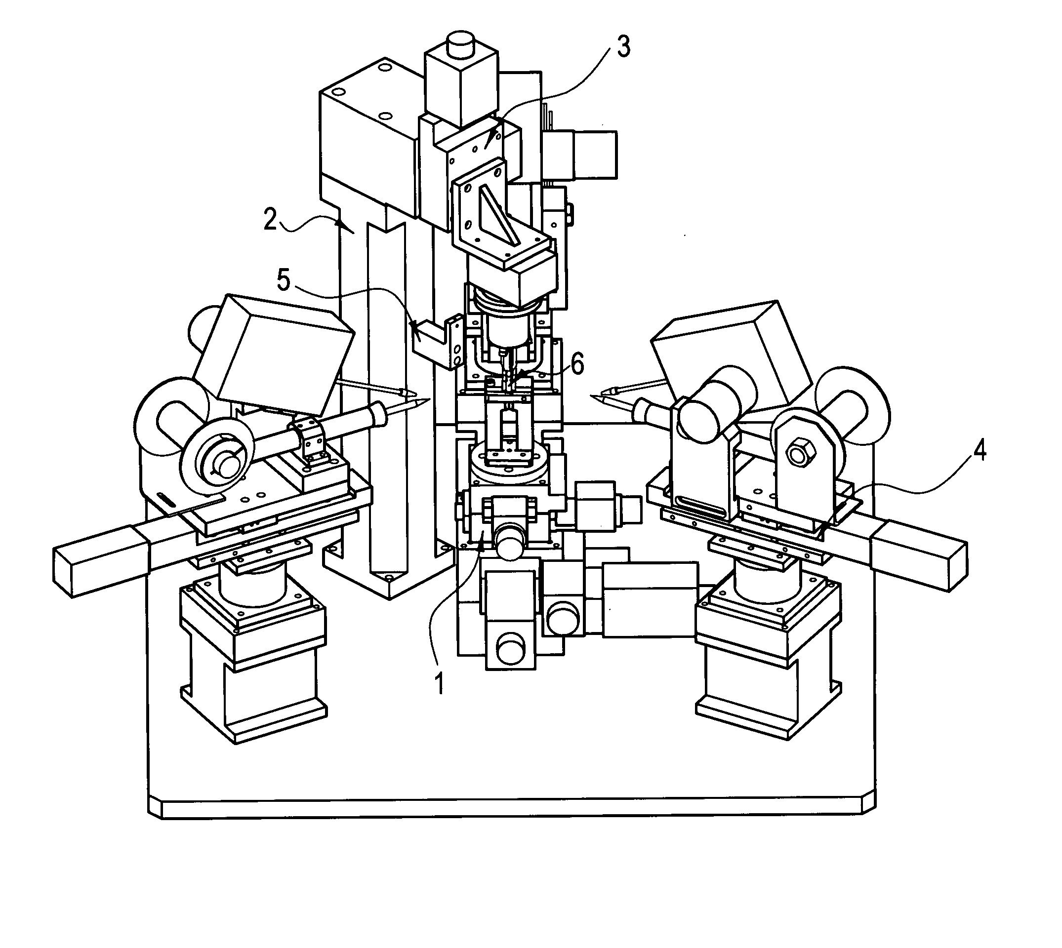
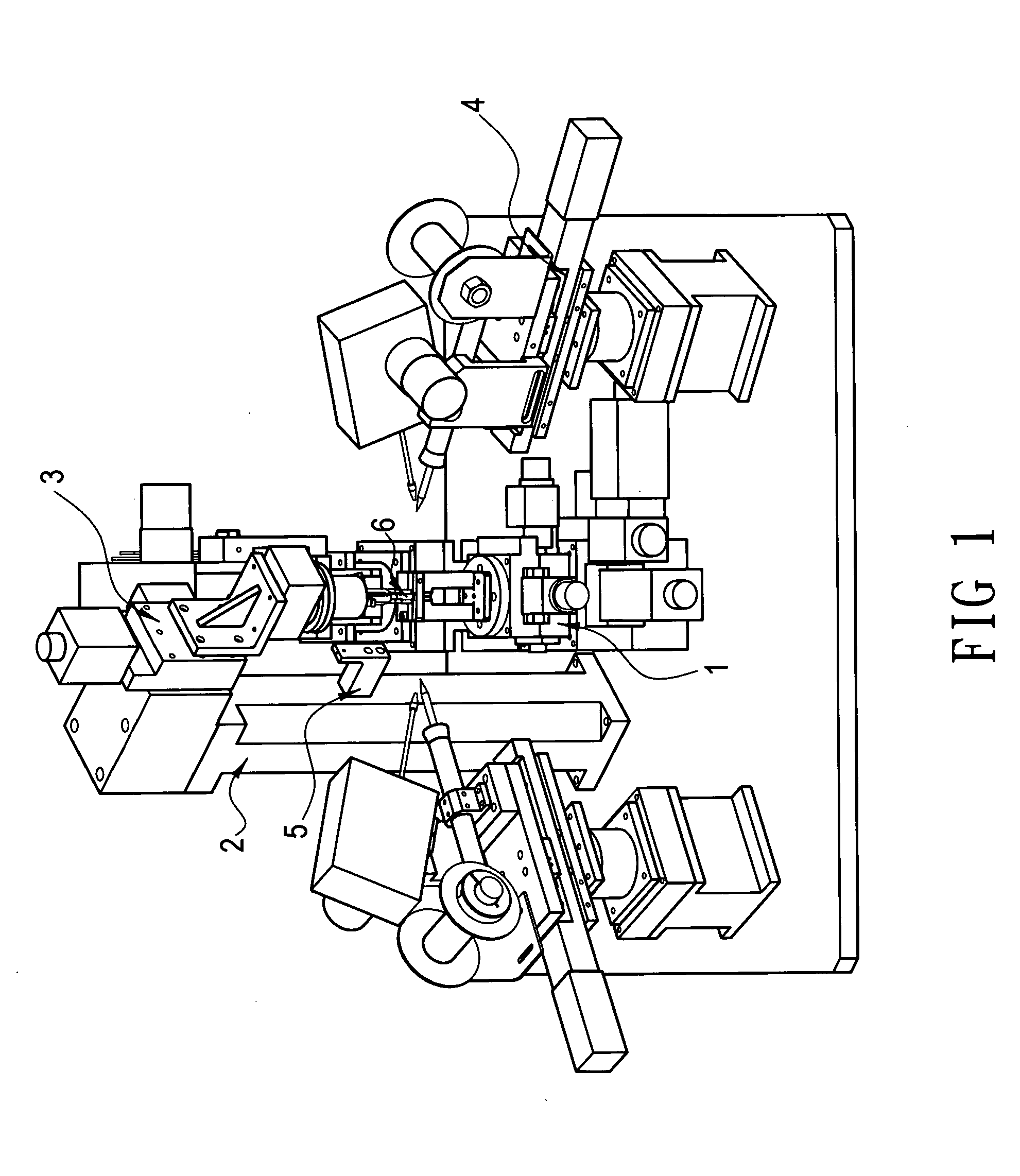
[0020] An automatic packaging apparatus of optical elements according to the present invention comprises a focusing platform set 1, a stud set 2, a Z-axis feeder set 3 and an automatic feeding set 4.

[0021] The focusing platform set 1, as shown in FIGS. 1 and 2, is provided thereon with a clamping tool 11.

[0022] The stud set 2, as shown in FIG. 1, is optionally provided with a photoelectric sensor 5 at a suitable location thereof.

[0023] The Z-axis feeder set 3 is ...


PUM

PropertyMeasurementUnit
included angleaaaaaaaaaa
distanceaaaaaaaaaa
depthaaaaaaaaaa

Abstract

An automatic packaging method of optical elements includes a focusing platform set, a Z-axis feeder set and an automatic feeding set. The Z-axis feeder set is provided above the focusing platform set. An automatic feeding set is arranged on a horizontal plane between the Z-axis feeder set and the focusing platform set by an appropriate distance. An upper part and a lower part of an optical element are supported by the lower end of the Z-axis feeder set and the upper end of the focusing platform set, respectively. The lower end of the Z-axis feeder set is adjusted vertically and horizontally with respect to the focusing platform set such that the upper part and the lower part are arranged in a line and coincide with each other. Afterward, by using the automatic feeding set, the upper part and the lower part of the optical element are bound together via the solders.

Description

BACKGROUND OF THE INVENTION [0001] 1. Field of the invention [0002] This invention relates to an automatic packaging apparatus and an automatic packaging method of optical elements, and in particular, to an apparatus and a method capable of automatically performing a focusing operation and automatically performing a welding operation. [0003] 2. Description of the Prior Art [0004] In the conventional processes, optical elements were packaged manually. The procedures associated with feeding, focusing, fixing and packaging operations are labor-intensive. Due to this limitation, high fabricating cost, low production and low yield adversely affect mass production of such optical elements and thus the development of their market scale is restricted. [0005] According to the conventional processes, tin solders were used as binders between the internal tube and the external tube. A solder stick was manually melted on a welding iron head, and then dropwise adhered on the wall of the internal ...

Claims


Application Information

Patent Timeline
Patent Type & Authority Applications(United States)
IPC IPC(8): B23K3/06
CPCB23K3/063
Inventor CHIEN, CHIH-HSIENCHIOU, SHEAN-SONTSAI, CHIN-YILIU, SUNG-HOTSENG, WEN-PENG
Owner IND TECH RES INST
Why Eureka
Try Eureka