Light emitting device, electronic appliance, and method for manufacturing light emitting device
- Summary
- Abstract
- Description
- Claims
- Application Information
AI Technical Summary
Benefits of technology
Problems solved by technology
Method used
Image
Examples
embodiment mode 1
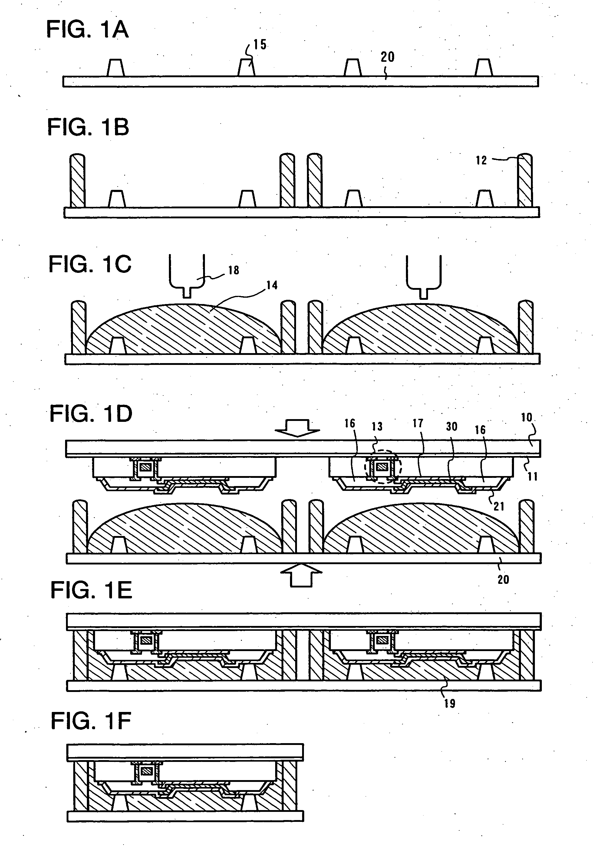
[0059] The present embodiment mode will explains a method for manufacturing a light emitting device in the case of the multiple pattern in which a pair of attached substrates is divided into multiple patterns (e.g., two pieces of panels are manufactured from a pair of attached substrates) with reference to FIGS. 1A to 1F.
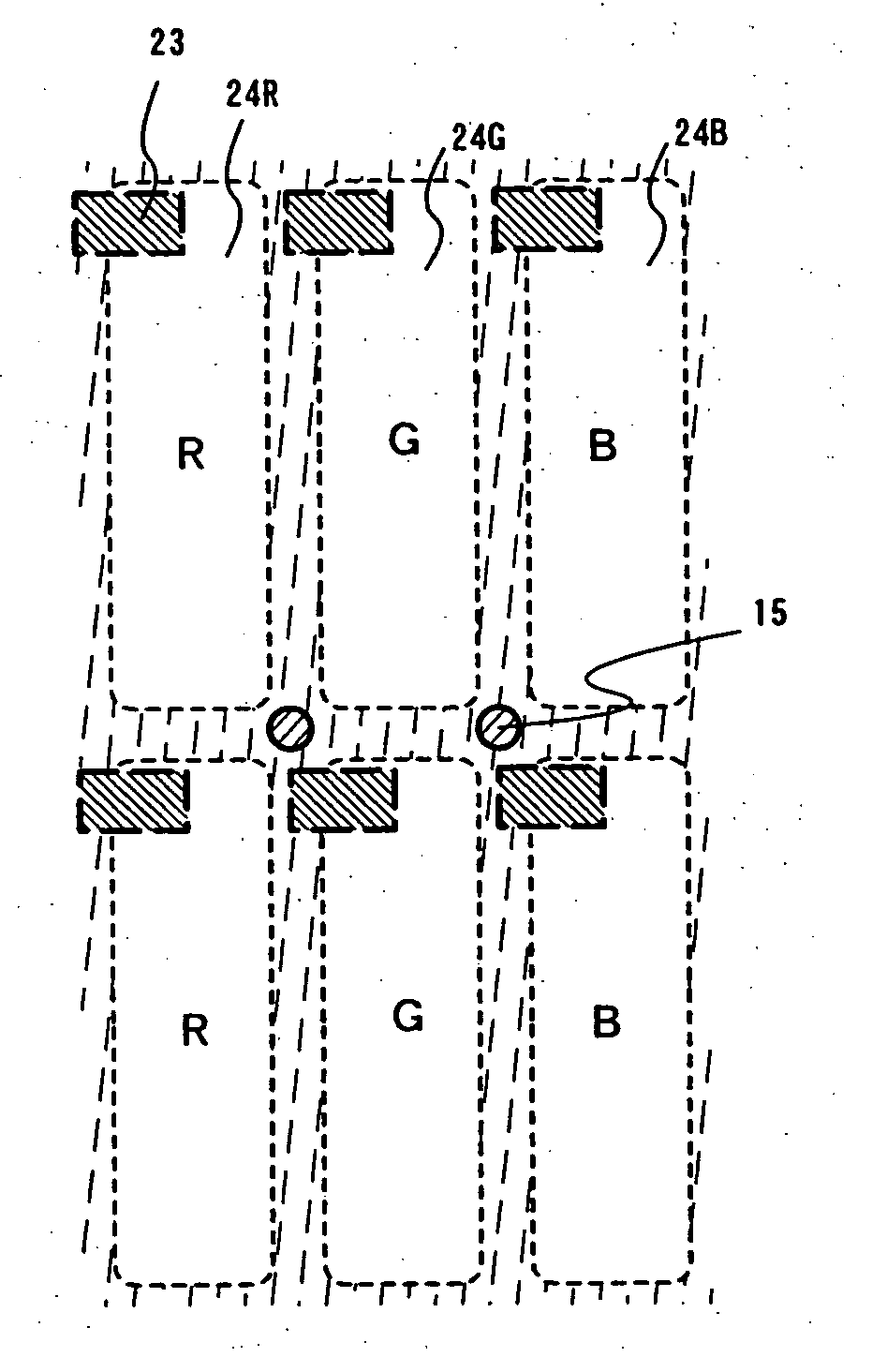
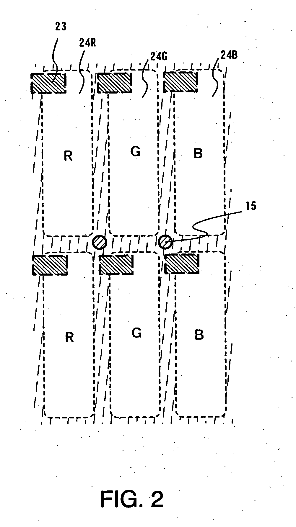
[0060] A second substrate 20 that will serve as a sealing substrate is prepared. Columnar spaces 15 are formed on the second substrate 20 (FIG. 1A). The columnar spacers 15 are formed by patterning a level film in predetermined portions. The height of the columnar spacers 15 is important, and determines a gap between two substrates. Although the columnar spacers are exemplified as structures for maintaining the gap therebetween, the spacers may have a wall-shaped structure or a grid-like structure, or a combination of such shapes.
[0061] The columnar spacers may contain a drying agent.
[0062] Patterns of a sealing material 12 is formed by using a dispenser device, ...
embodiment mode 2
[0078] A method for manufacturing a dual-emission type display device will be described with reference to FIG. 5.
[0079] A base insulating film is formed on a substrate 400. In order to extract light from the substrate 400 as a display screen, a substrate with a light transmitting property such as a glass substrate and a quartz substrate may be used as the substrate 400. A heat-resistant plastic substrate with a light transmitting property that can withstand a processing temperature can also be employed. A glass substrate is, herein, used as the substrate 400. The refractive index of the glass substrate is approximately 1.55.
[0080] As the base insulating film, a base film made from a silicon oxide film, a silicon nitride film, a silicon oxynitride film, and the like is formed. The base insulating film has light transmitting properties. Although the base insulating film has, herein, two-layer structure, it may have a single layer or two or more layers of the above insulating films. ...
embodiment 1
[0132] In the present embodiment, FIG. 8 shows an example of a manufacturing device that is partly different of those in FIGS. 6 and 7.
[0133] As well as FIG. 6 and FIG. 7, the manufacturing device as shown in FIG. 8 includes: the transport chamber 108 for transporting a substrate to the delivery chamber 111; the delivery chamber 107; the gates 100j, and 100n to 100s; and the film formation chambers 109, 110, 113, and 132. In the embodiment, the portions identical to those in FIG. 6 and FIG. 7 will not be further explained for the sake of simplification. To prevent moisture from adhering, an inert gas (e.g., nitrogen gas) having a controlled dew point is preferably filled in the chambers (including the delivery chamber, the processing chamber, the transport chamber, a film formation chamber, etc.), other than an unloading chamber 219 and a sealing substrate loading chamber 217. Preferably, pressure in such chambers filled with an inert gas is kept under reduced pressure.
[0134] In F...
PUM
 Abstract
Description
Claims
Application Information


