Semiconductor memory device for reducing current consumption in operation

a memory device and silicon-based technology, applied in the field of silicon-based silicon-based memory devices, can solve problems such as unnecessary current consumption, and achieve the effect of reducing unnecessary current consumption in its operation

Active Publication Date: 2005-06-30
SK HYNIX INC
View PDF3 Cites 8 Cited by
  • Summary
  • Abstract
  • Description
  • Claims
  • Application Information

AI Technical Summary

Benefits of technology

[0028] It is, therefore, an object of the present invention to provide a synchronous memory device for reducing unnecessary current consumption in its operation.

Problems solved by technology

Consequently, this can leads unnecessary current consumption.

Method used


Image

  • Semiconductor memory device for reducing current consumption in operation
  • Semiconductor memory device for reducing current consumption in operation
  • Semiconductor memory device for reducing current consumption in operation

Examples


Embodiment Construction

[0037] Hereinafter, a data output control circuit for use in a semiconductor memory device in accordance with the present invention will be described in detail referring to the accompanying drawings.

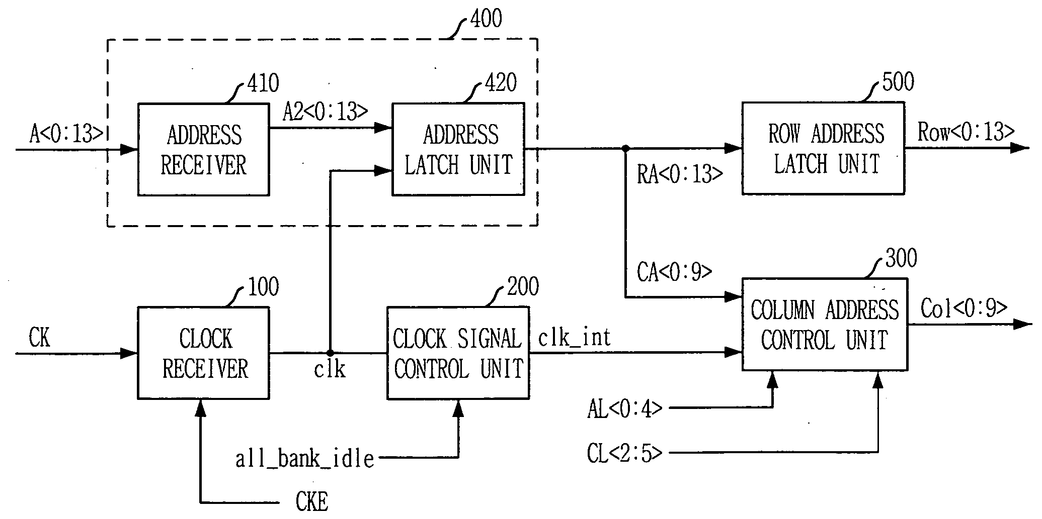
[0038]FIG. 2 provides a block diagram of a semiconductor memory device in accordance with a preferred embodiment of the present invention.

[0039] Referring to FIG. 2, the synchronous memory device of the embodiment includes a clock receiver 100 for receiving an external clock CK to output a first internal clock clk; an address receiver 410 for receiving and transferring an address A; an address latch unit 420 for latching the address A2 that is transferred by the address receiver 410, in synchronous with the first internal clock clk; a row address latch unit 500 for latching a row address RA that is outputted from the address latch unit 420 to output an inner row address Row; a column address control unit 200 for buffering the first internal clock clk to output a second internal clock c...


PUM


Abstract

A synchronous memory device can reduce unnecessary current consumption in its operation. In the synchronous memory device, a clock receiver receives an external clock to output a first internal clock. An address latch unit receives and latches an address in synchronous with the first internal clock. A row address latch unit latches a row address that is outputted from the address latch unit. A column address control unit receives the first internal clock to output a second internal clock and stops the output of the second internal clock when a non-column command is performed. Finally, a column address control unit is activated in response to the second internal clock to count a column address that is outputted from the address latch unit so as to output an inner column address.

Description

FIELD OF INVENTION [0001] The present invention relates to a semiconductor memory device; and, more particularly, to a semiconductor memory device capable of reducing current consumption in its operation. DESCRIPTION OF PRIOR ART [0002] A semiconductor memory device has been continuously improved to increase its operational speed with increased integration. There has been introduced, so called, a synchronous memory device which operates in synchronous with an external clock signal, so as to improve the operational speed of the semiconductor memory device. [0003] The synchronous semiconductor memory device performs a data access operation at the rising edge of the external clock signal. That is, the synchronous semiconductor memory device can perform the data access operation once within one cycle of the external clock signal. Such a synchronous semiconductor memory device that performs the data access operation once within one cycle of the external clock signal is particularly calle...

Claims


Application Information

Patent Timeline
Patent Type & Authority Applications(United States)
IPC IPC(8): G11C11/40G11C7/10G11C7/22G11C8/18
CPCG11C7/1072G11C7/22G11C11/418G11C8/18G11C7/222G11C11/40
Inventor KANG, SHIN-DEOKKWEAN, KI-CHANG
Owner SK HYNIX INC
Why Eureka
Try Eureka