
Magnetic memory
- Summary
- Abstract
- Description
- Claims
- Application Information
AI Technical Summary
Benefits of technology
Problems solved by technology
Method used
Image

Examples
first embodiment
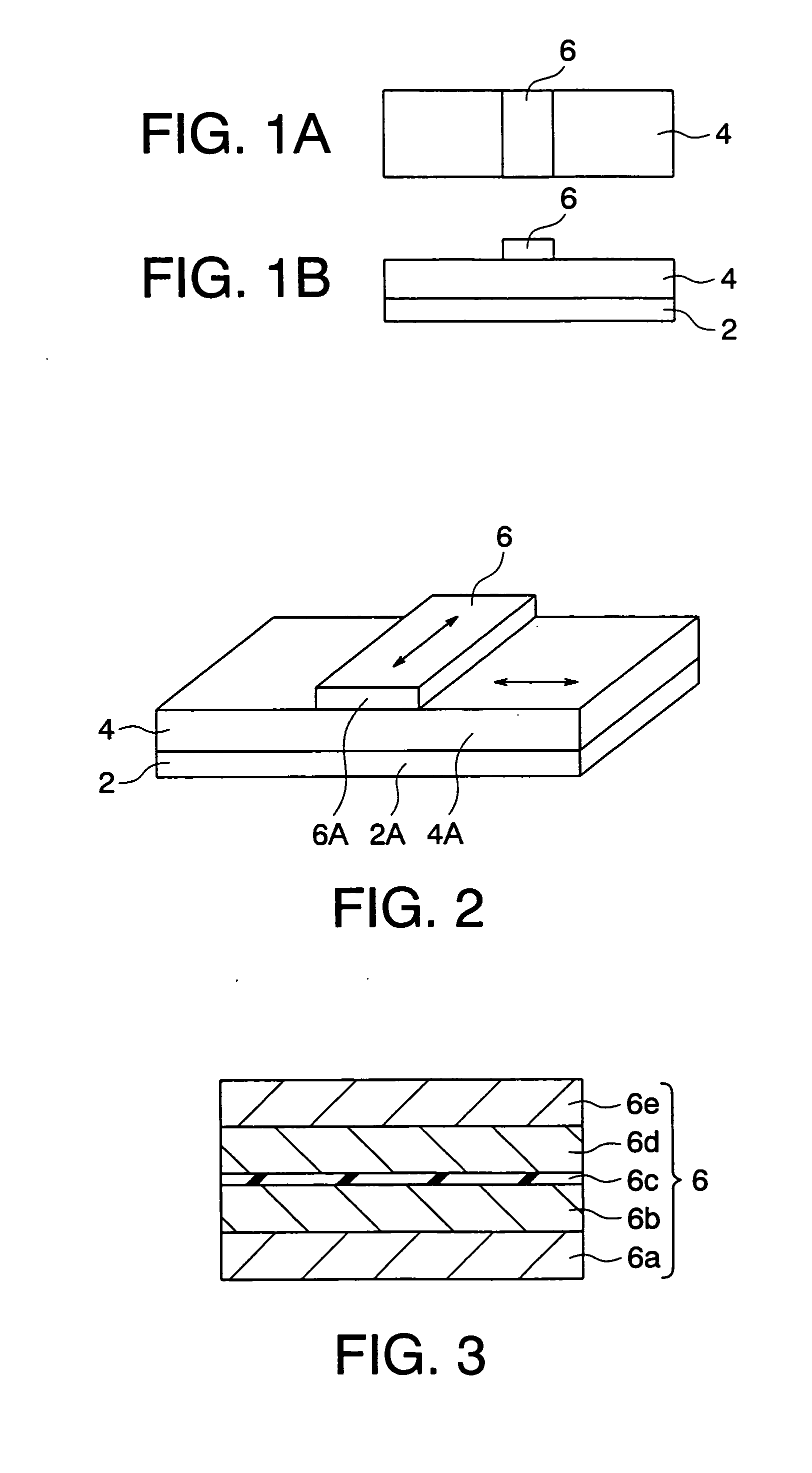
[0077] A magnetic memory according to a first embodiment of the present invention will be explained with reference to FIG. 1A to FIG. 11. A magnetic memory according to this embodiment has a plurality of memory cells arranged in a matrix array. A constitution of each memory cell is schematically shown in FIGS. 1A and 1B. FIGS. 1A and 1B are a plan view and a front view of a memory cell according to the embodiment, respectively. FIG. 2 is a perspective view of the memory cell according to the embodiment. The memory cell according to the embodiment is provided with a TMR element 6, a writing wire 4 for performing writing on the TMR element 6, and a yoke 2 formed of a magnetic layer. The writing wire 4 is formed on the yoke 2, and the TMR element 6 is formed on the writing wire 4. Incidentally, a wire (not shown) used for reading is provided on the TMR element 6.
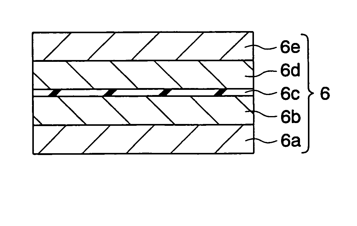
[0078] As shown in FIG. 3, for example, the TMR element 6 has a stacking structure of a lower electrode layer 6a, a magnetiz...
second embodiment
[0102] Next, a constitution of a memory cell in a magnetic memory according to a second embodiment of the present invention is schematically shown in FIG. 12. The memory cell in the magnetic memory according to the embodiment is constituted such that, for example, a barrier metal layer 3 with a film thickness of 10 nm made of Ta has been inserted between the wire 4 connected to the TMR element 6 constituting the memory cell and the yoke 2 in the magnetic memory of the first embodiment. By inserting the barrier metal 3, mutual diffusion between material constituting a composition element for the wire 4, for example, Cu or Al, and material constituting the yoke 2, for example, permalloy (Ni—Fe) can be prevented from occurring. As the barrier metal, any one of TaN, TiN and WN can be used besides Ta. A barrier metal layer may be provided between the yoke 2 and a base substrate 100.
[0103] The magnetic memory of the embodiment can also reduce writing current without causing fluctuation o...
third embodiment
[0104] Next, a constitution of a memory cell of a magnetic memory according to a third embodiment of the present invention is schematically shown in FIG. 13.
[0105] In the first and second embodiments, writing is performed by turning on two transistors to cause current to flow in only in the wire 4. At that time, magnetic field required for reversing magnetization of the magnetization free layer 6b of the TMR element 6 serves as a coercive force in a direction of an easy magnetization axis of the TMR element 6.
[0106] The third embodiment of the present invention has a constitution that another wire 14 is formed on the TMR element 6 so as to be perpendicular to the wire 4 (refer to FIG. 13). In this embodiment, writing can be performed utilizing asteroid characteristic of the TMR element 6 by causing current to flow in the wire 4 and the wire 14 simultaneously, and writing current is further reduced.
[0107] Next, a method for manufacturing the magnetic memory according to the embodi...
PUM
 Abstract
Description
Claims
Application Information