

Method for fabricating MOS-FET
a field effect transistor and mosfet technology, applied in the direction of transistors, electrical devices, semiconductor devices, etc., can solve the problems of reduced maximum depleted layer width, difficult formation of fully depleted type transistors, and difficult application of methods to fully depleted type soi having a thin soi layer with the thickness of 50 nm or less, etc., to achieve enhanced diffusion, high throughput, and increase the effect of threshold valu
- Summary
- Abstract
- Description
- Claims
- Application Information
AI Technical Summary
Benefits of technology
Problems solved by technology
Method used
Image

Examples
Embodiment Construction
[0035]In the following detailed description of the preferred embodiments, reference is made to the accompanying drawings which form a part hereof, and in which is shown by way of illustration specific preferred embodiments in which the inventions may be practiced. These preferred embodiments are described in sufficient detail to enable those skilled in the art to practice the invention, and it is to be understood that other preferred embodiments may be utilized and that logical, mechanical and electrical changes may be made without departing from the spirit and scope of the present inventions. The following detailed description is, therefore, not to be taken in a limiting sense, and scope of the present inventions is defined only by the appended claims.
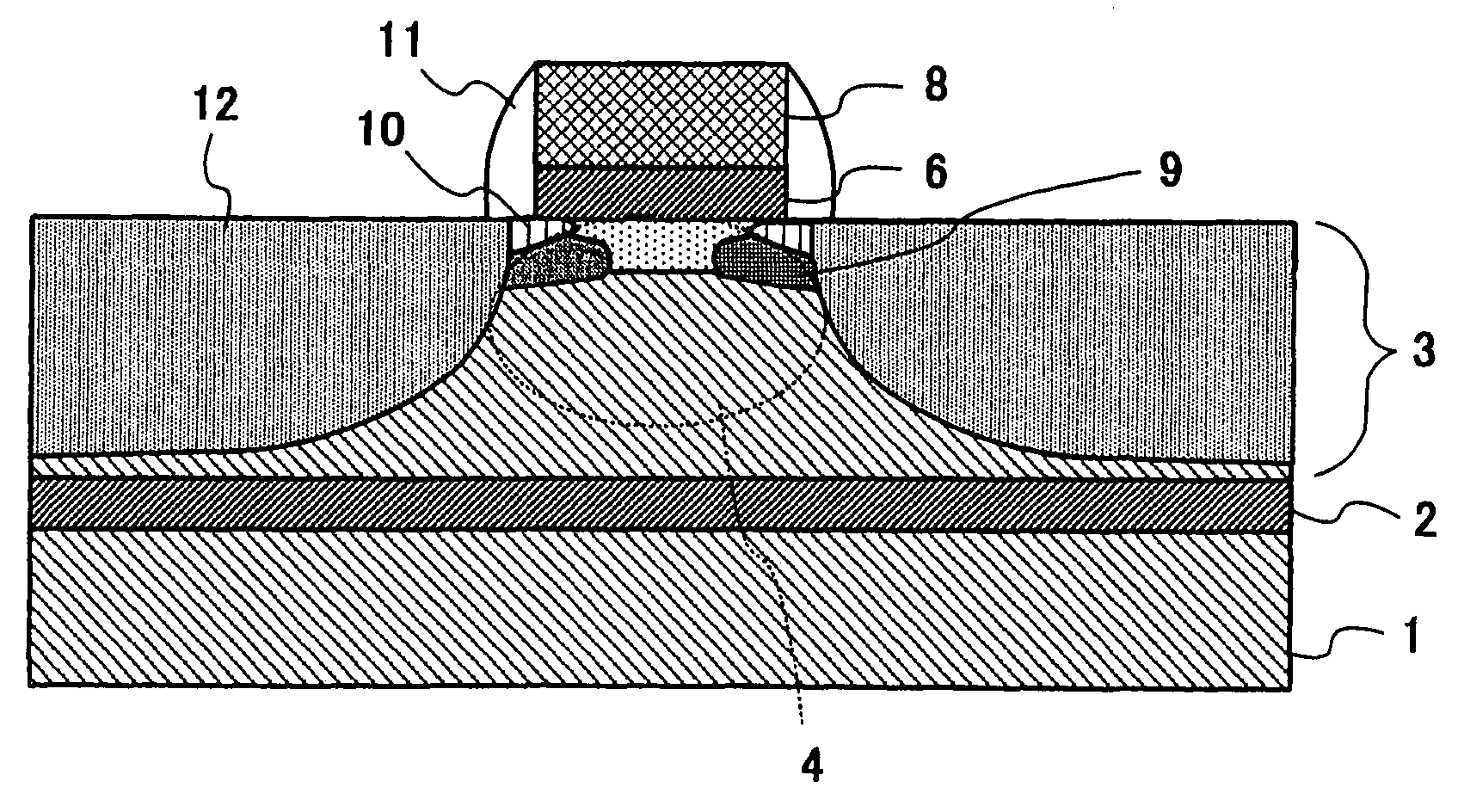
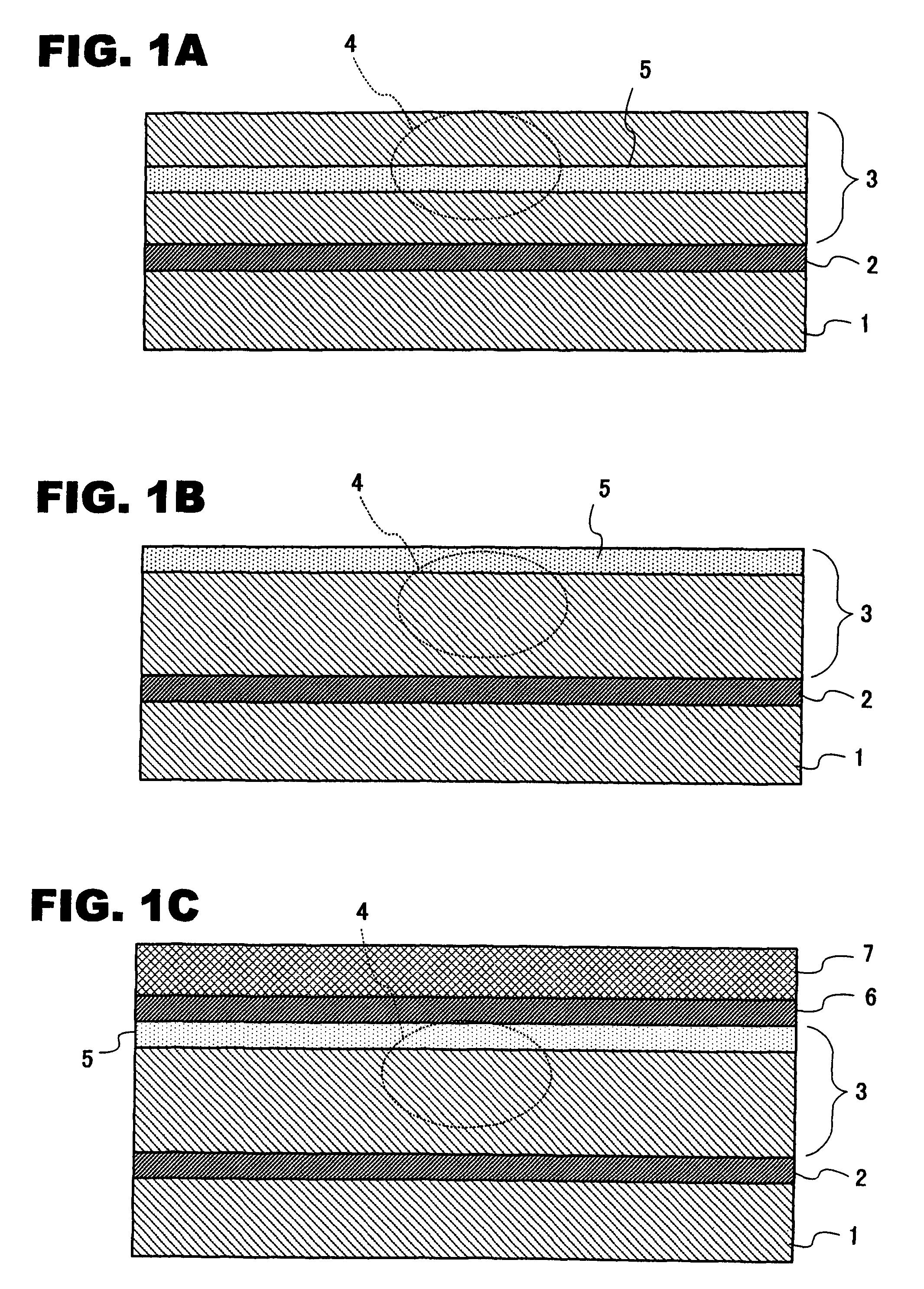
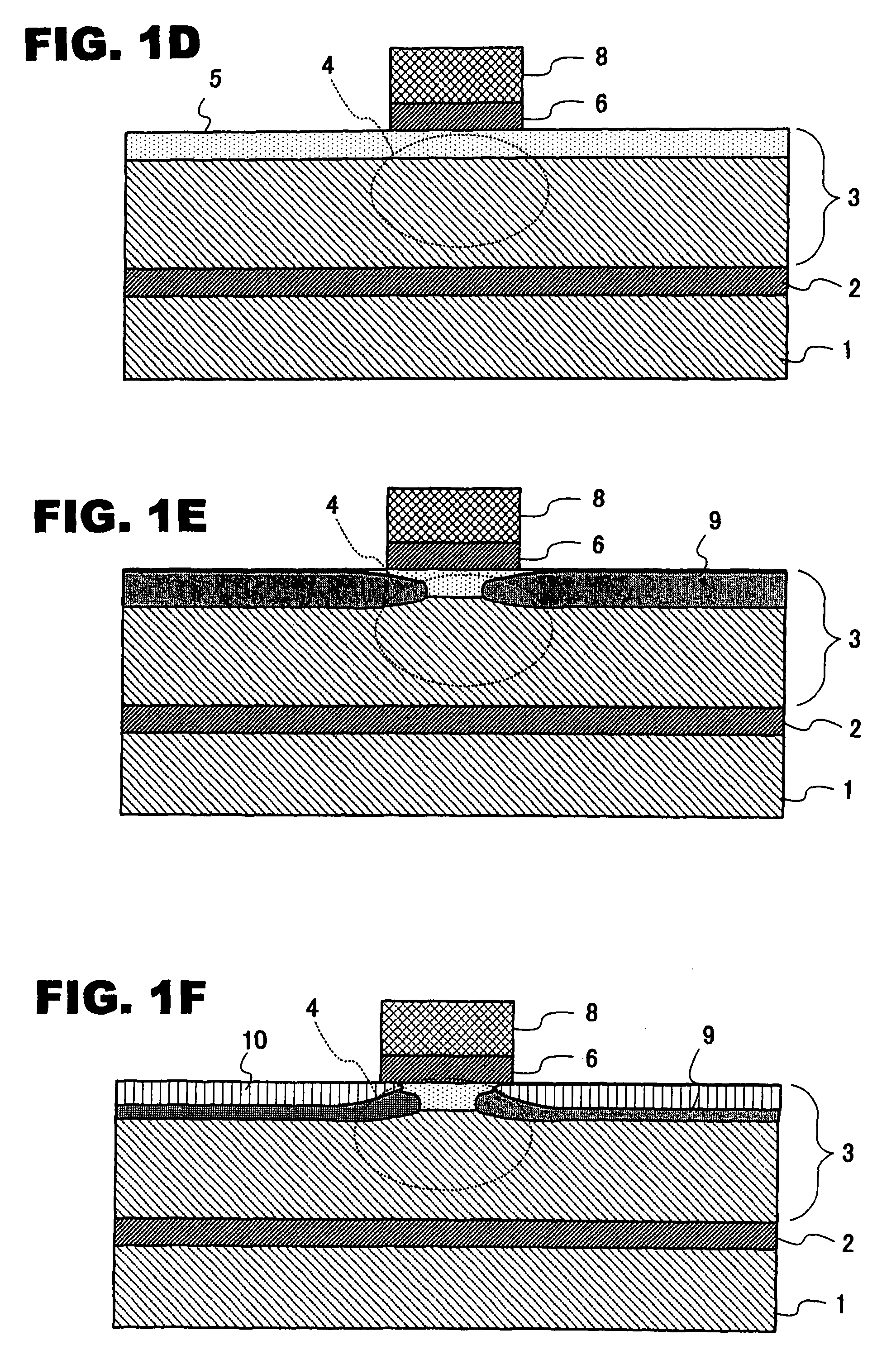
[0036]The present invention will be described referring to an embodiment illustrated below. FIGS. 1A to 1H show an essential part of a method for fabricating a semiconductor device of the present invention. A buried oxide film 2 and a...
PUM
| Property | Measurement | Unit |
|---|---|---|
| thickness | aaaaa | aaaaa |
| thickness | aaaaa | aaaaa |
| temperature | aaaaa | aaaaa |
Abstract
Description
Claims
Application Information