High mobility enhancement mode FET

a high-mobility enhancement and transistor technology, applied in the field of semiconductor structure, can solve the problems of increasing the threshold voltage variation to unacceptable levels, short-channel effects, and expected increase in threshold voltage variation, and achieves the effects of effective reduction of impurity and surface scattering phenomena, reducing random dopant fluctuation phenomena, and high doping profiles

Active Publication Date: 2014-08-12
QUALCOMM INC
View PDF20 Cites 102 Cited by
  • Summary
  • Abstract
  • Description
  • Claims
  • Application Information

AI Technical Summary

Benefits of technology

[0023]The present invention describes a transistor which has a MOSFET like structure, with the difference that the device channel is formed in an intrinsic region, so as to effectively decrease the impurity and surface scattering phenomena deriving from an high doping profile into the channel typical of conventional MOS devices. Due to the presence of the un-doped channel region, the proposed structure greatly reduces Random Dopant Fluctuation phenomena drastically decreasing the threshold voltage variation between different devices. In order to control the threshold voltage of the device, an heavily doped poly-silicon or metallic gate is used. However, differently from standard CMOS devices, a high work-function metallic material, or a heavily p-doped poly-silicon layer, is used for an n-channel device and a low work-function metallic material, or heavily n-doped poly-silicon layer, is used for a p-channel FET. Retrograde doping and / or halo implants are used in order to control the Short Channel Effects.
[0024]In order to better understand this concept, let us consider the structure illustrated in FIG. 1, which represents one of the embodiments of the present invention in CMOS technology. As it can be seen, conventional device terminals (source, gate and drain) are present. However the channel region under the gate oxide is made intrinsic (or near-intrinsic) allowing for an improvement of the carrier mobility.
[0025]The electrons in the channel are free to move with a reduced impurity scattering and their confinement at the channel surface is lowered, allowing for a notable improvement in the charge transport (since the transport becomes partially bulk, reducing the surface scattering phenomena).

Problems solved by technology

This aggressive trend poses several technology and circuit design challenges.
One such challenge is the expected increase in threshold voltage variation due to worsening Short Channel Effect (SCE) and Random Dopant Fluctuation (RDF).
The highly non-uniform profile sets up a higher effective doping concentration toward shorter devices, which counteracts short-channel effects.
Therefore, super-halo profiles, or similar techniques (such as retrograde doping), do not eliminate issues related with random dopant density fluctuations, which can increase the threshold voltage variation to unacceptable levels.
Such fluctuations may seriously affect the functionality, performance, and yield of the corresponding systems.
Another important limitation related to high channel doping is the degradation of the carrier mobility associated with the impurity scattering and quantum confinement phenomena that take place in the device channel.
These phenomena reduce the drive current in the device heavily degrading the device performance.
However, this advantage comes at the cost of an increase of the short channel effects, such as punch-through phenomena.
This solution, even if very effective to reduce SCE, requires a much more complex and costly manufacturing process involving Silicon On Insulator technology, which is still quite expensive nowadays.
A second problem is the alignment of the different gates of the device.
Furthermore, since they are built on buried oxide, they cannot be used for power applications, since their capability to dissipate heat is very poor.
Finally, since these devices operate in fully-depleted mode, they do not have the intrinsic body diodes typical of conventional bulk MOS devices.
This characteristic limits the range of applications suitable for these technologies.
This configuration unfortunately is not practical, since it can be used only for an array of MOSFET connected all in parallel.
Since the threshold voltage is adjusted varying the body voltage, each transistor not connected in parallel must be built in an isolated well adding to the silicon area and therefore to the cost of the solution.
Unfortunately also this solution, suffers of the same drawbacks of the previous one, since the body voltage must differ between various devices.
Furthermore, since the channel region has been n-doped, the RDF phenomena still causes high threshold voltage variation in the process flow.
Although the cited prior art references describe structures that present an enhanced carrier mobility, they are not very practical to be used in modern integrated circuits, where it is impossible to separately bias the body terminal of each device without increasing their leakage current and forming separated wells for each of them.

Method used


Image

  • High mobility enhancement mode FET
  • High mobility enhancement mode FET
  • High mobility enhancement mode FET

Examples


Embodiment Construction
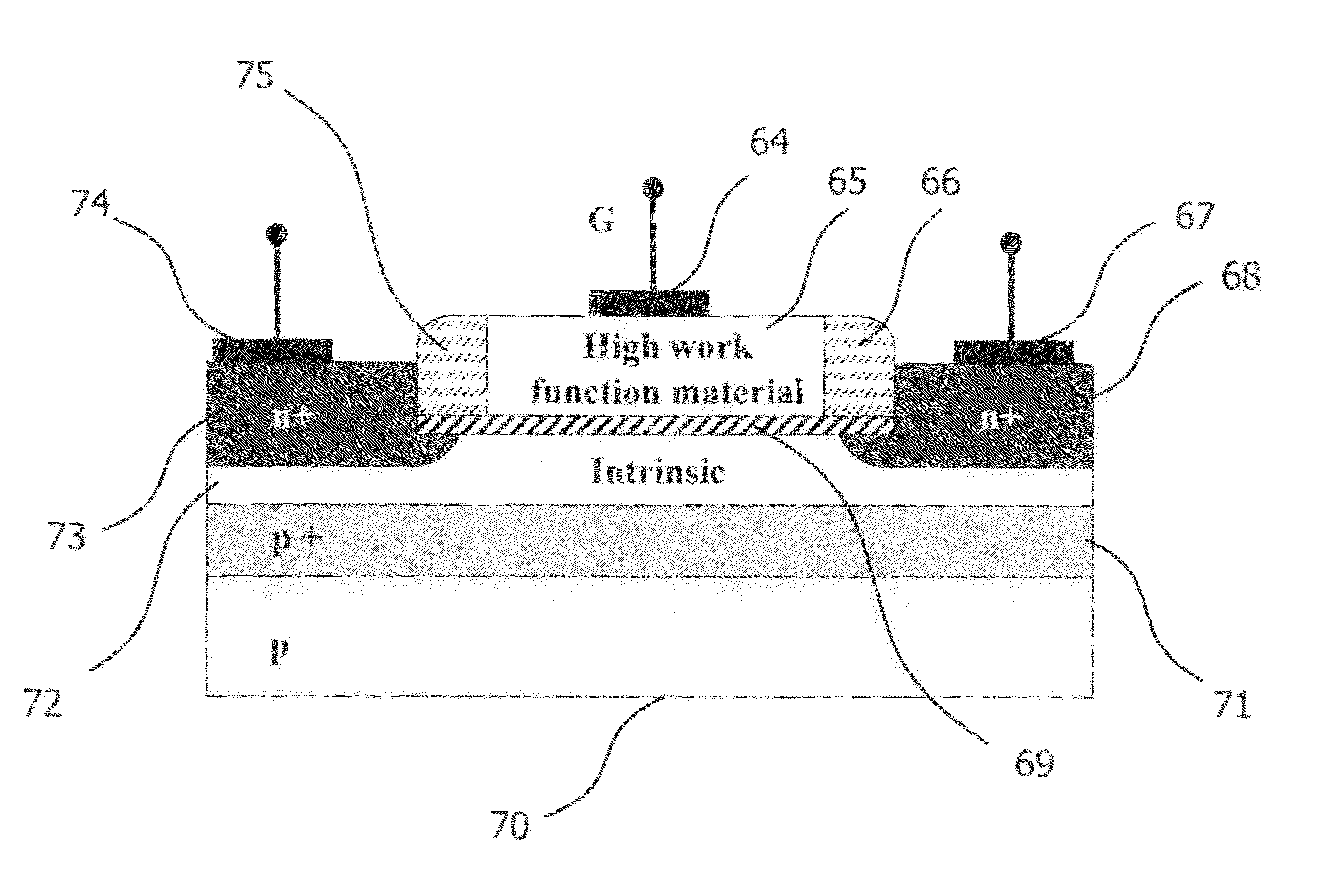
A FIG. 1

[0075]FIG. 1 is showing the first general embodiment of the invention. Regions 4 and 7, which can be made in n+-type semiconductor or metal, define the drain and the source of the transistor. The region 9 corresponds to the gate-oxide, and the region 5 is the p-type substrate of the device. The gate electrode 2, which can be built in metal or poly-silicon, forms the gate of the transistor. As it can be seen, differently from a conventional MOS device where the channel region is p-doped and the gate is made in n+-doped poly-silicon or with a low work-function metallic material, the channel region 6 of this embodiment is kept intrinsic, and the gate 2 is formed with a high work-function material.

[0076]The present invention therefore defines a MOS device with a higher carrier mobility, which leads to a significant improvement of the device performance. Since the channel region is substantially un-doped, the impurity scattering and the surface roughness scattering phenomena are ...


PUM


Abstract

A novel semiconductor transistor is presented. The semiconductor structure has a MOSFET like structure, with the difference that the device channel is formed in an intrinsic region, so as to effectively decrease the impurity and surface scattering phenomena deriving from a high doping profile typical of conventional MOS devices. Due to the presence of the un-doped channel region, the proposed structure greatly reduces Random Doping Fluctuation (RDF) phenomena decreasing the threshold voltage variation between different devices. In order to control the threshold voltage of the device, a heavily doped poly-silicon or metallic gate is used. However, differently from standard CMOS devices, a high work-function metallic material, or a heavily p-doped poly-silicon layer, is used for a n-channel device and a low work-function metallic material, or heavily n-doped poly-silicon layer, is used for a p-channel FET.

Description

BACKGROUND OF THE INVENTION[0001]1. Field of the Invention[0002]The present invention is in the field of semiconductor structures. The present invention is further in the field of semiconductor structures of transistor devices. The present invention further relates to the field of integrated devices and circuits. The implementation is not limited to a specific technology, and applies to either the invention as an individual component or to inclusion of the present invention within larger systems which may be combined into larger integrated circuits.[0003]2. Brief Description of Related Art[0004]The driving force for the semiconductor industry growth has been the elegant scaling nature of CMOS technology. This aggressive trend poses several technology and circuit design challenges. One such challenge is the expected increase in threshold voltage variation due to worsening Short Channel Effect (SCE) and Random Dopant Fluctuation (RDF).[0005]Nevertheless, with proper control of the dop...

Claims


Application Information

Patent Timeline
Patent Type & Authority Patents(United States)
IPC IPC(8): H01L21/70H01L21/8234H01L27/088H01L29/10H01L29/423H01L29/49H01L29/51H01L29/66H01L29/78
CPCH01L27/0886H01L29/4236H01L29/4916H01L29/105H01L29/1083H01L29/7833H01L21/823431H01L29/7851H01L29/66628H01L29/517H01L29/66621
Inventor MARINO, FABIO ALESSIOMENEGOLI, PAOLO
Owner QUALCOMM INC
Why Eureka
Try Eureka