Electric device having nanowires, manufacturing method thereof, and electric device assembly

a technology of electric devices and nanowires, applied in the direction of nanotechnology, semiconductor devices, electrical equipment, etc., can solve the problems of large-scale manufacturing facilities and huge apparatus, compound semiconductor transistors have limited uses, and the cost reduction and process simplification are problems to be solved

Inactive Publication Date: 2007-06-07
CANON KK
View PDF3 Cites 96 Cited by
  • Summary
  • Abstract
  • Description
  • Claims
  • Application Information

AI Technical Summary

Benefits of technology

[0037] According to the present invention, characteristics of an electric device using nanowires can be modified by cutting or changing electric characteristics of the nanowires. An electric device having nanowires, which is high-performance, can thus be manufactured through a simple, low-cost process in a large area. The present invention also makes it possible to modify characteristics of an electric device that employs nanowires and reduce characteristics fluctuations even when sophisticated nanowire arranging techniques are not available. Applied to active matrix displays, imaging devices, phase-coherent antennas, and the like, the electric device using nanowires improves the performance of these appliances.
[0038] When using a TFT device in which nanowires serve as conductive channels, the use of nanowires has the following additional effect.
[0039] A TFT device using nanowires can be trimmed while maintaining characteristics of the TFT device, unlike conventional TFT devices, which are rendered completely nonfunctional by trimming. Laser trimming, which is not usable in conventional TFT devices, is thus made employable and various advantages of laser trimming can now be utilized.

Problems solved by technology

However, silicon-based transistors need a large-scale manufacturing facility and a huge apparatus for film formation in the device fabrication process through chemical vapor deposition, or other similar film forming methods, at high temperature under vacuum.
Accordingly, cost reduction and process simplification are problems to be solved.
Despite those diversity of characteristics, compound semiconductor transistors have limited uses since their materials are expensive and their device fabrication process is a large-scale, complicated process comparable to that of silicon-based transistors described above.
However, organic transistors are significantly low in carrier mobility (up to 0.1 cm2 / Vs), which determines the performance of a transistor, compared to that of silicon-based transistors, and are said to require significant progress with regard to material and manufacture process for being applicable to various electronic devices.
As described, none of the prior art TFT devices has succeeded in having high transistor performance and in being obtainable by a simple, low-cost device fabrication process, and development of such a transistor has been desired.
However, simply applying a nanowire solution to a substrate is not enough and has to be accompanied by orientation / arrangement control of each nanowire.
Laser trimming cannot be performed on TFT devices since it only makes TFT devices physically unusable.
On the other hand, the simple process allows nanowires to be arranged irregularly, which leads to characteristics fluctuations.

Method used


Image

  • Electric device having nanowires, manufacturing method thereof, and electric device assembly
  • Electric device having nanowires, manufacturing method thereof, and electric device assembly
  • Electric device having nanowires, manufacturing method thereof, and electric device assembly

Examples


first embodiment

[0060] A first embodiment of the present invention is described with reference to FIGS. 1 to 6.

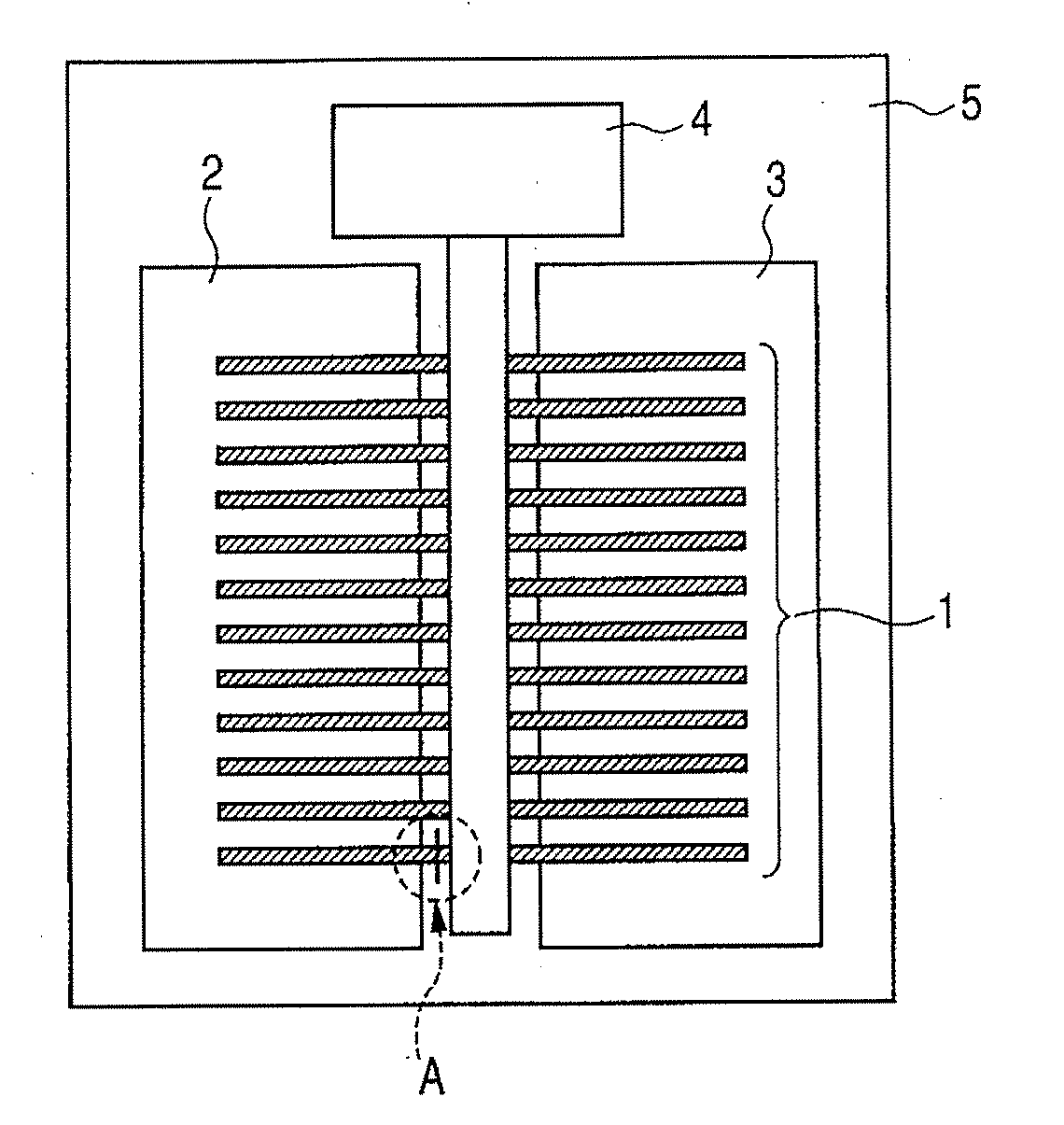
[0061]FIG. 1 is a schematic diagram of a nanowire TFT according to this embodiment. In FIG. 1, Reference Numeral 1 denotes nanowires composed of a semiconductor material, ‘2’ denotes a source electrode, ‘3’, a drain electrode, ‘4’, a gate electrode, and ‘5’, a glass substrate.

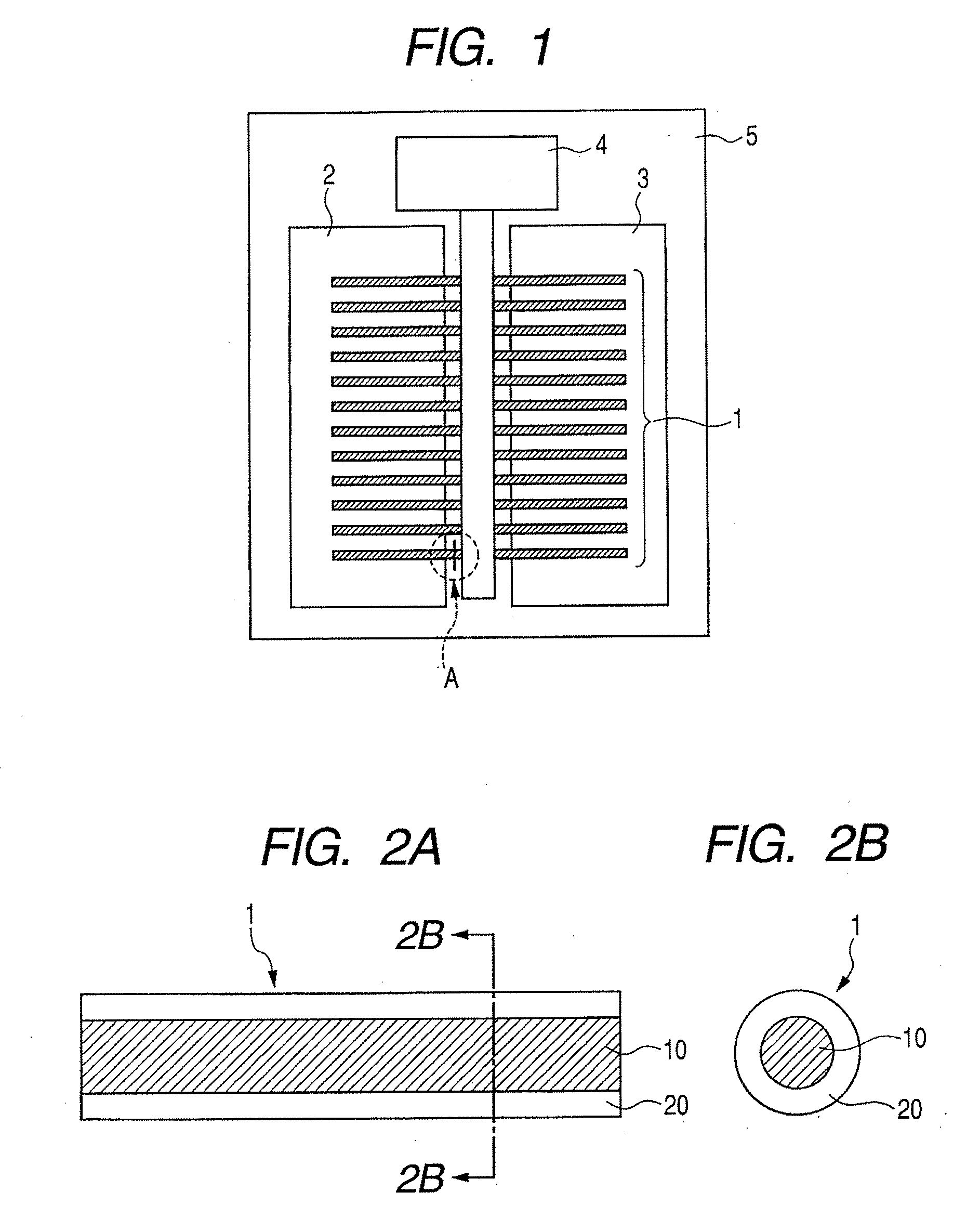
[0062] The nanowire 1 is a wire-shaped component with a diameter of several nm to several hundreds nm and a length of several μm to one hundred μm (aspect ratio: 10 to 104). The nanowire 1 can have other shapes than the wire shape, including a tube shape like a carbon nanotube.

[0063] The semiconductor material of the nanowire 1 can be one selected from or a combination of Group IV semiconductors (C, Si, Ge, Sn). Group III-V semiconductors (Al, Ga, In) (N, P, As, Sb) and Group II-VI semiconductors (Be, Mg, Zn, Cd, Hg) (O, S, Se, Te) can also be employed. Also employable are combinations of the above semiconductors w...

second embodiment

[0085] A second embodiment of the present invention is next described with reference to FIG. 6.

[0086] In the first embodiment, a case in which characteristics of a TFT device are modified when the arrangement of the nanowires 1 is ideal is described. In contrast, this embodiment deals with a case in which characteristics of a TFT device are modified when the arrangement of the nanowires 1 is irregular.

[0087]FIG. 6 is a schematic diagram of a TFT device having nanowires according to this embodiment. In FIG. 6, Reference Numeral 1 denotes nanowires formed from a semiconductor material; ‘2’, a source electrode; ‘3’, a drain electrode; ‘4’, a gate electrode; and ‘5’, a glass substrate. The structure and manufacturing method of the TFT device in the second embodiment are the same as in the first embodiment.

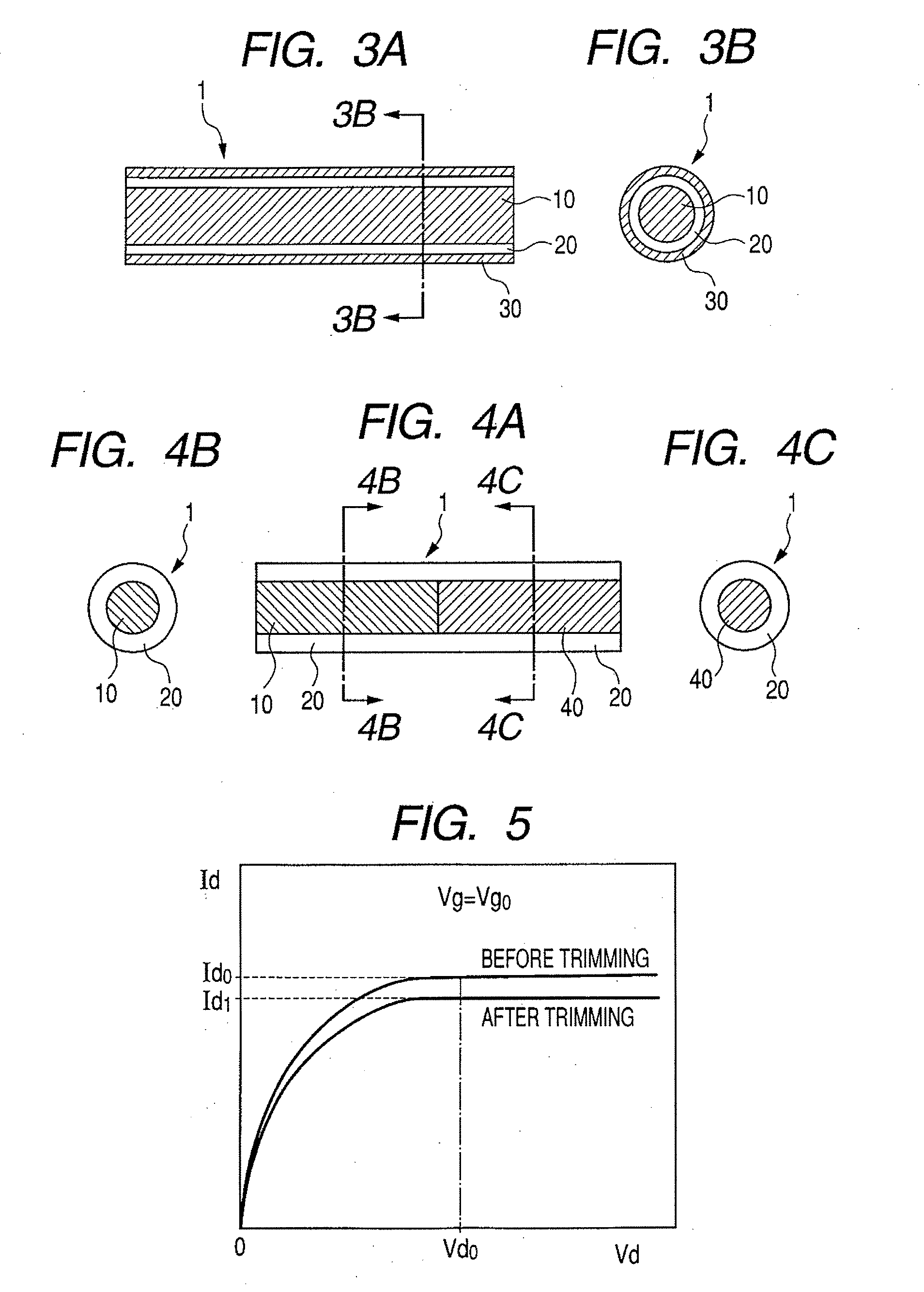
[0088] The example of FIG. 6 shows a case in which the value of a characteristic is degraded mainly by a defective arrangement of the nanowires 1. For instance, the channel length o...

third embodiment

[0093] A third embodiment of the present invention is described next with reference to FIGS. 7 and 8.

[0094] This embodiment is an application of the present invention to a nanowire TFT device assembly (an electric device assembly) in which a plurality of nanowire TFT devices structured as described in the above embodiments are arranged on the same substrate.

[0095] A nanowire TFT device assembly shown in FIG. 7 constitutes a display portion of a substrate for an active matrix liquid crystal display. Switching devices having nanowire TFT devices (electric devices) 200 are two-dimensionally fabricated on a substrate 10 along row and column directions. The TFT devices 200 each have the same structure as that of the above-described nanowire TFT, and a description thereof is omitted here.

[0096]FIG. 8 shows the frequency distribution of the mutual conductance of each nanowire TFT device 200 illustrated in FIG. 7. FIG. 8 shows a change in characteristic distribution before and after nano...


PUM


Abstract

An electric device having a plurality of nanowires, in which at least one of the nanowires is cut or changed in its electric characteristics so as to have a desired characteristic value of the electric device.

Description

BACKGROUND OF THE INVENTION [0001] 1. Field of the Invention [0002] The present invention relates to an electric device having nanowires, a method of manufacturing such electric device, and an electric device assembly. In particular, the present invention relates to an electric device such as a TFT device that uses nanowires as conductive channels, and a method of manufacturing such electric device. [0003] 2. Description of the Related Art [0004] A thin film transistor (TFT) is a switching device used in various electronic devices. Known transistor devices that constitute the TFT include silicon-based transistors (single crystal, polycrystal, and amorphous), compound semiconductor transistors (III-V group, II-VI group, and IV-IV group), and organic transistors (low molecular, and polymer). [0005] Of those, silicon-based transistors, which use silicon for a semiconductor layer, have the following characteristics: [0006] 1) Their material, silicon, is infinitely abundant on the surfac...

Claims


Application Information

Patent Timeline
Patent Type & Authority Applications(United States)
IPC IPC(8): H01L29/76
CPCB82Y10/00H01L29/0665H01L29/0673H01L29/78675H01L29/78681H01L29/78684H01L29/7869H01L29/78696H01L51/0017H01L51/0048H01L51/0545Y10S977/938H10K71/231H10K85/221H10K10/466
Inventor IKEDA, SOTOMITSU
Owner CANON KK
Why Eureka
Try Eureka