Method for fabricating interconnections with carbon nanotubes

a technology of carbon nanotubes and interconnections, which is applied in the direction of electrical equipment, semiconductor devices, semiconductor/solid-state device details, etc., can solve the problems of electrical migration and rc delay, difficult to have a good connection interface and an appropriate contact, and achieves low contact resistance , simple and low-cost fabrication process, the effect of enhancing the growth of carbon nanotubes

Inactive Publication Date: 2013-06-11
NATIONAL TSING HUA UNIVERSITY
View PDF8 Cites 3 Cited by
  • Summary
  • Abstract
  • Description
  • Claims
  • Application Information

AI Technical Summary

Benefits of technology

[0006]Another objective of the present invention is to provide a method which avoids a complicated semiconductor fabrication process, protects the metal interface from being oxidized, and prevents the resistance from increasing.
[0011]In the present invention, the carbon nanotubes are grown between a catalytic layer and an upper covering layer through a chemical vapor deposition method. The upper covering layer protects the catalytic layer from being oxidized and enhances the growth of the carbon nanotubes. Since the carbon nanotubes are respectively connected with the lower substrate and the upper conductive wire via the catalytic layer and the upper covering layer, they have relatively low contact resistance. Furthermore, the upper covering layer can function as a metal barrier layer, and prevent metal from spreading to other materials via diffusion or other approaches. The present invention also features a simple and low-cost fabrication process.

Problems solved by technology

As the circuit density increases and the size of the semiconductor decreases, the spacing between the metal wires is consistently reduced, which introduces the problems of electrical migration and RC delay.
However, it is usually difficult to have a good connection interface and an appropriate contact resistance between a metal wire and a carbon nanotube structure.
However, such a structure increases the number of fabrication steps.

Method used


Image

  • Method for fabricating interconnections with carbon nanotubes
  • Method for fabricating interconnections with carbon nanotubes
  • Method for fabricating interconnections with carbon nanotubes

Examples


Embodiment Construction

[0015]The embodiments and technical contents of the present invention are described in detail along with the drawings below.

[0016]Refer to FIGS. 1A-1F and FIG. 2. FIGS. 1A-1F are schematic diagrams showing a method for fabricating interconnections with carbon nanotubes according to one embodiment of the present invention. FIG. 2 is a flowchart of a method for fabricating interconnections with carbon nanotubes according to one embodiment of the present invention. The present invention proposes a method for fabricating interconnections with carbon nanotubes, which comprises steps of:

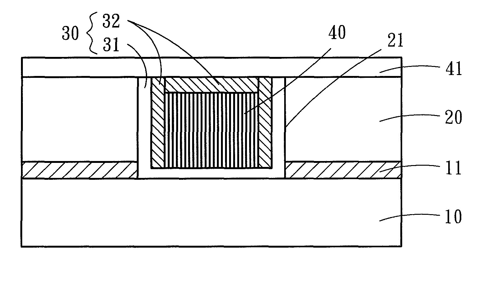
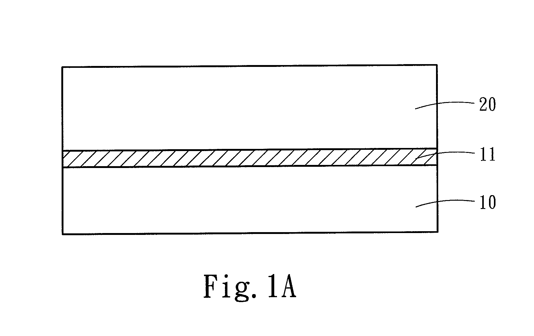
[0017]Step S1: forming an etch stop layer 11 on a substrate 10. The substrate 10 is made of a conductive material, such as copper. The etch stop layer 11 is made of a non-conductive material and may function as a copper-diffusion barrier layer. The etch stop layer 11 is made of silicon nitride in one embodiment.

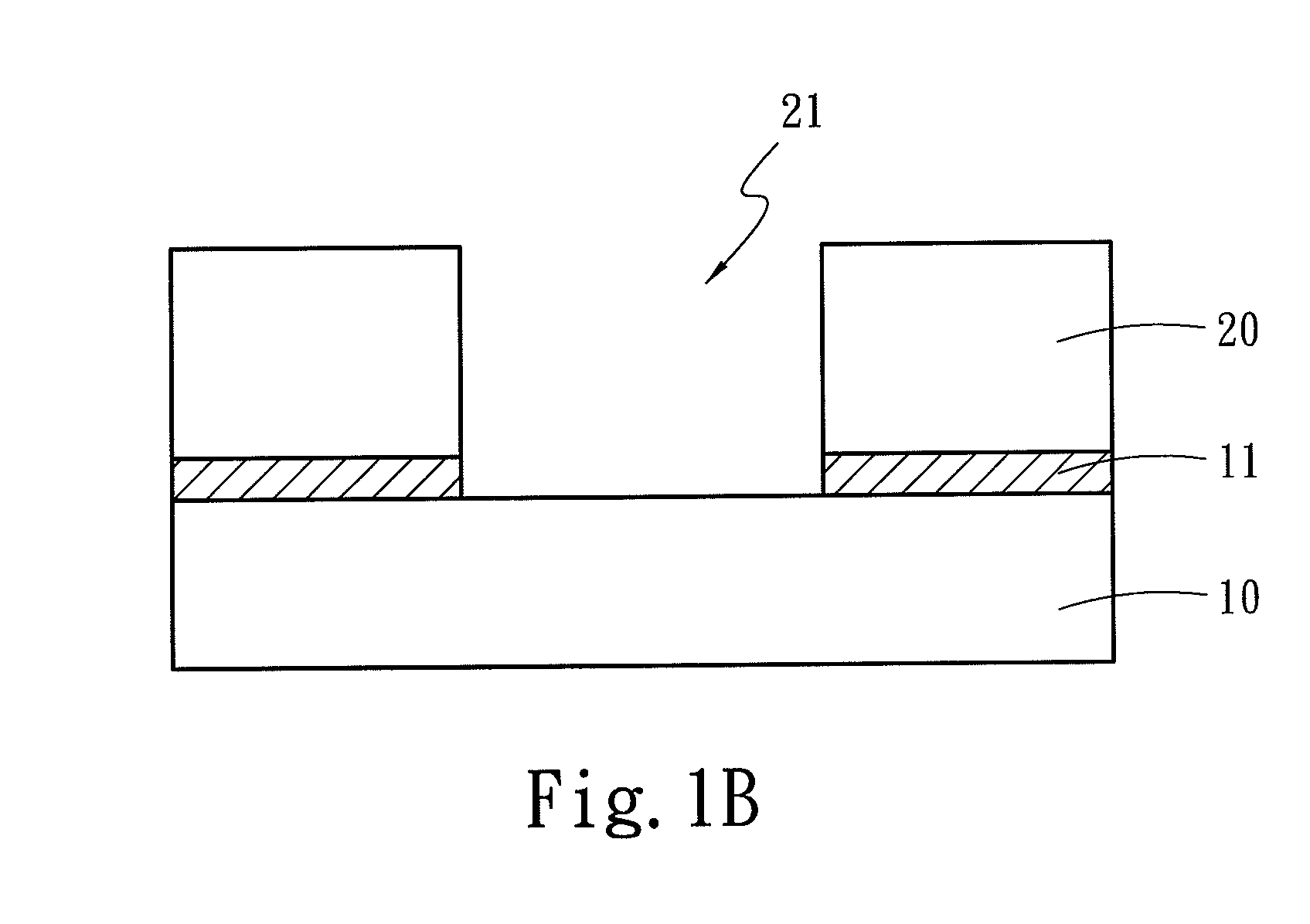
[0018]Step S2: forming an insulating layer 20 on the substrate 10 and forming a hole 21 on the i...


PUM

PropertyMeasurementUnit
conductiveaaaaaaaaaa
permittivityaaaaaaaaaa
circuit densityaaaaaaaaaa

Abstract

A method for fabricating interconnections with carbon nanotubes of the present invention comprises the following steps: forming a dual-layer that contains a catalytic layer and an upper covering layer on the periphery of a hole connecting with a substrate; and growing carbon nanotubes on the catalytic layer with the upper covering layer covering the carbon nanotubes. The present invention grows the carbon nanotubes between the catalytic layer and the upper covering layer. The upper covering layer protects the catalytic layer from being oxidized and thus enhances the growth of the carbon nanotubes. The carbon nanotubes are respectively connected with the lower substrate and an upper conductive wire via the catalytic layer and the upper covering layer, which results in a lower contact resistance. Moreover, the upper covering layer also functions as a metal-diffusion barrier layer to prevent metal from spreading to other materials via diffusion or other approaches.

Description

FIELD OF THE INVENTION[0001]The present invention relates to a method for fabricating carbon nanotubes, particularly to a method for fabricating interconnections with carbon nanotubes.BACKGROUND OF THE INVENTION[0002]As the circuit density increases and the size of the semiconductor decreases, the spacing between the metal wires is consistently reduced, which introduces the problems of electrical migration and RC delay. Usually, a carbon nanotube structure can be used to solve the abovementioned problems. However, it is usually difficult to have a good connection interface and an appropriate contact resistance between a metal wire and a carbon nanotube structure.[0003]R.O.C. patent No. I298520 disclosed a “Method for Electroplating an Interconnection Containing a Carbon Nanotube and Metal Composite Material”, wherein a substrate with an interconnection formed on the surface is electroplated in an electroplating bath containing metal ions and carbon nanotubes to form a conductive wir...

Claims


Application Information

Patent Timeline
Patent Type & Authority Patents(United States)
IPC IPC(8): H01L21/00
CPCH01L21/76849H01L21/76876H01L21/76879H01L23/53276H01L2924/0002H01L2221/1094H01L2924/00
Inventor WU, HSIN-WEITSAI, CHUNG-MINYEW, TRI-RUNG
Owner NATIONAL TSING HUA UNIVERSITY
Why Eureka
Try Eureka