Semiconductor memory device for dynamically storing data with channel body of transistor used as storage node

a memory device and transistor technology, applied in semiconductor devices, digital storage, instruments, etc., can solve the problems of unreasonable design of semiconductor devices, increased manufacturing costs, and reduced manufacturing yields

Inactive Publication Date: 2005-06-30
KK TOSHIBA
View PDF8 Cites 152 Cited by
  • Summary
  • Abstract
  • Description
  • Claims
  • Application Information

AI Technical Summary

Problems solved by technology

Further, it is expected that the structure is miniaturized in future, the capacitor structure and manufacturing process become unavoidably complicated, and therefore, a problem that the manufacturing yield is lowered and the manufacturing cost rises will occur.
However, in the conventional semiconductor memory device disclosed in Jpn. Pat. Appln. KOKAI Publication No. 2002-343886 and the like, the design thereof becomes unreasonable in order to attain a cell area of 4F2 (F is determined by a design rule).
As a result, there occurs a possibility that data disturbance (information destruction) occurs.
Further, since the high-impurity concentration layer of part of the channel body portion lies adjacent to the source and drain, the junction leak current increases and the retention characteristic may be deteriorated.

Method used


Image

  • Semiconductor memory device for dynamically storing data with channel body of transistor used as storage node
  • Semiconductor memory device for dynamically storing data with channel body of transistor used as storage node
  • Semiconductor memory device for dynamically storing data with channel body of transistor used as storage node

Examples


first embodiment

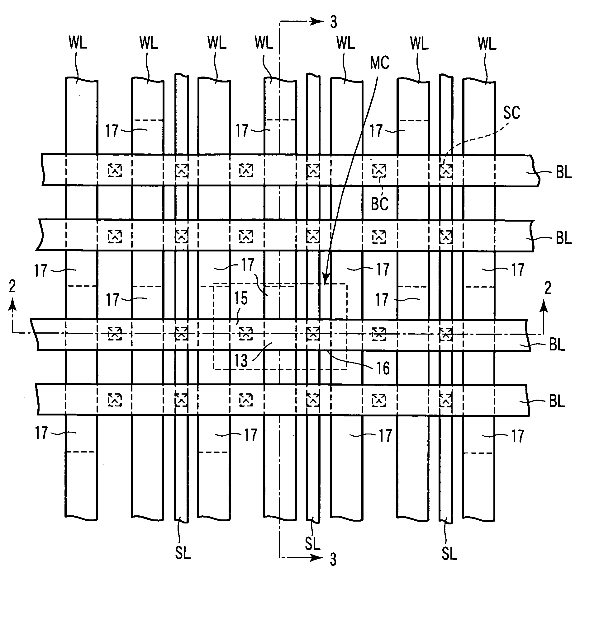
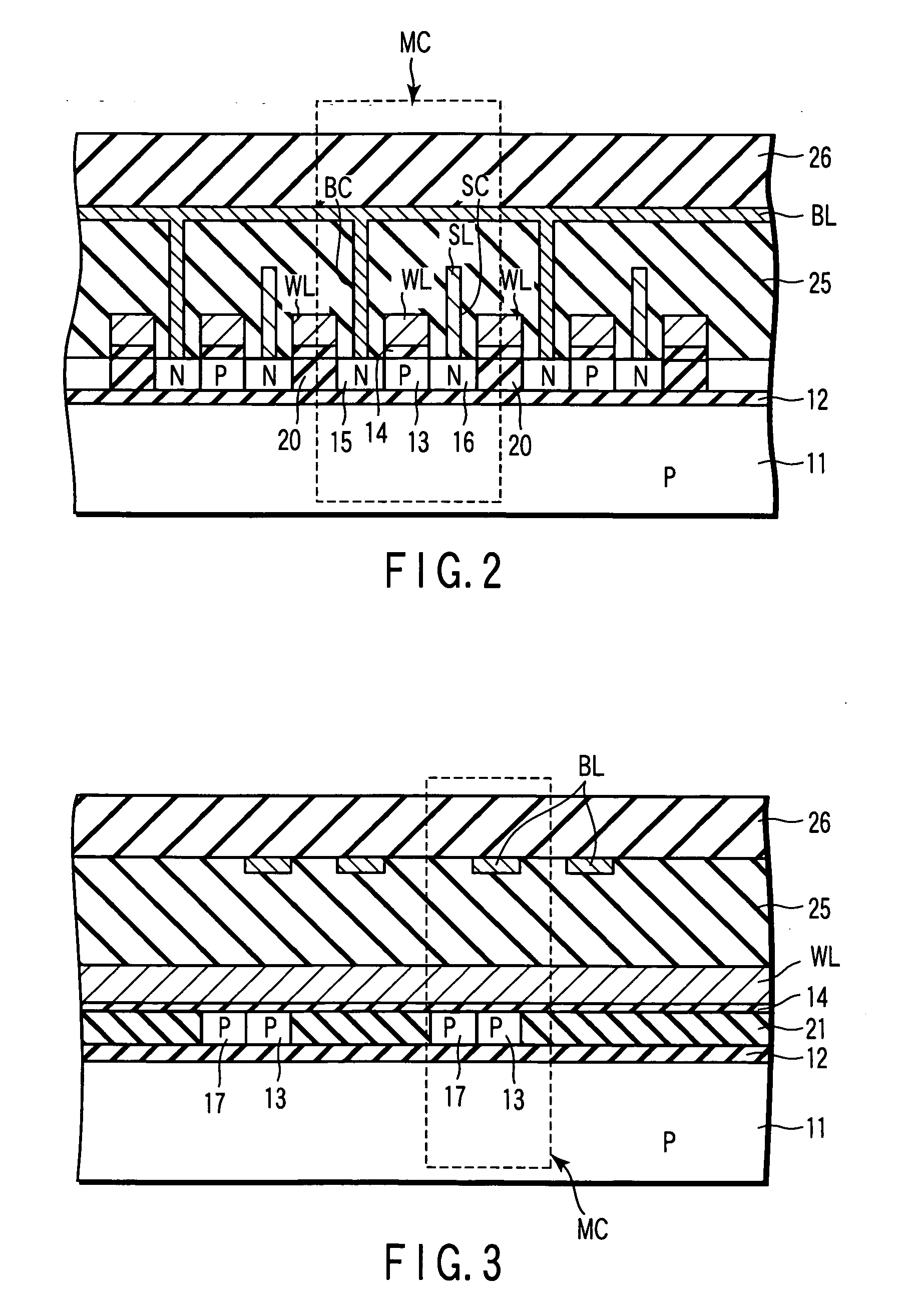
[0040] First, a semiconductor memory device according to a first embodiment of this invention is explained with reference to FIGS. 1 to 3. The semiconductor memory device shown in FIGS. 1 to 3 is a so-called floating body cell (FBC) device and is a DRAM cell which uses the channel body of a transistor as a storage node to recognize data based on a difference in the current-voltage characteristic of the transistor caused by the potential of the storage node.

[0041]FIG. 1 is a plan view schematically showing one example of a memory cell array of the semiconductor memory device according to the first embodiment. FIG. 2 is a cross-sectional view taken along the 2-2 line of FIG. 1 and viewed in the arrow direction. FIG. 3 is a cross-sectional view taken along the 3-3 line of FIG. 1 and viewed in the arrow direction.

[0042] A portion surrounded by broken lines in FIG. 1 indicates a memory cell MC of one bit unit. The memory cells MC are respectively provided at intersections of word lines...

second embodiment

[0063] Next, a semiconductor memory device according to a second embodiment of this invention is explained with reference to FIGS. 4 to 6. In the following explanation, the repetitive explanation for the same portion as that of the first embodiment is omitted.

[0064]FIG. 4 is a plan view schematically showing one example of the semiconductor memory device according to the second embodiment. FIG. 5 is a cross-sectional view taken along the 5-5 line of FIG. 4 and viewed in the arrow direction. FIG. 6 is a cross-sectional view taken along the 6-6 line of FIG. 4 and viewed in the arrow direction.

[0065] As shown in FIGS. 4 to 6, memory cells MC are arranged at intersections of first word lines WL1 and bit lines BL. The memory cell MC surrounded by broken lines in FIG. 4 indicates one bit unit and the cell size is 16F2. Second word lines WL2 are arranged adjacent to the respective first word lines WL1 and formed to extend in the above direction. In other words, adjacent word lines of one...

third embodiment

[0074] Next, a semiconductor memory device according to a third embodiment of this invention is explained with reference to FIGS. 7 to 9. In the following explanation, the repetitive explanation for the same portion as that of the first and second embodiments is omitted.

[0075]FIG. 7 is a plan view schematically showing one example of the semiconductor memory device according to the third embodiment. FIG. 8 is a cross-sectional view schematically showing the semiconductor memory device taken along the 8-8 line of FIG. 7 and viewed in the arrow direction. FIG. 9 is a cross-sectional view schematically showing the semiconductor memory device taken along the 9-9 line of FIG. 7 and viewed in the arrow direction.

[0076] As shown in FIGS. 7 to 9, memory cells MC are arranged at intersections of first word lines WL1 and bit lines BL. The memory cell MC surrounded by broken lines in FIG. 7 indicates one bit unit and the cell size is 12F2. Second word lines WL2 and dummy word lines DL are ar...


PUM


Abstract

A semiconductor memory device includes a plurality of MIS transistors arranged at intersections of first word lines and bit lines formed on an SOI substrate and each configuring a memory cell. Each of the plurality of MIS transistors includes a channel body formed in a semiconductor layer on an insulating film and set in an electrically floating state, a first extension region formed in contact with the channel body in the semiconductor layer and arranged in a first word line direction, a gate insulating film formed on the channel body, a gate electrode formed on the gate insulating film and electrically connected to a corresponding one of the first word lines, and source and drain regions separately formed in a bit line direction in the semiconductor layer to sandwich the channel body.

Description

CROSS-REFERENCE TO RELATED APPLICATIONS [0001] This application is based upon and claims the benefit of priority from prior Japanese Patent Application No. 2003-433930, filed Dec. 26, 2003, the entire contents of which are incorporated herein by reference. BACKGROUND OF THE INVENTION [0002] 1. Field of the Invention [0003] This invention relates to a semiconductor memory device and more particularly to a semiconductor memory device including floating body cells (FBCs) each of which dynamically stores data with the channel body of a transistor used as a storage node. [0004] 2. Description of the Related Art [0005] Conventionally, a general dynamic random access memory (DRAM) which is used as a memory with high integration density contains memory cells each of which is configured by one metal oxide semiconductor (MOS) transistor and one capacitor. Further, for example, an static random access memory (SRAM) contains memory cells each of which is configured by four or six MOS transistor...

Claims


Application Information

Patent Timeline
Patent Type & Authority Applications(United States)
IPC IPC(8): G11C11/24H01L27/108G11C11/404H01L21/8239H01L21/8242H01L21/84H01L27/105H01L27/12
CPCH01L21/84H01L27/105H01L27/108H01L27/1052H01L29/7841H01L29/785H01L27/1203H10B99/00H10B12/00
Inventor YAMADA, TAKASHIHORIGUCHI, FUMIOOHSAWA, TAKASHIIWATA, YOSHIHISAASAO, YOSHIAKI
Owner KK TOSHIBA
Why Eureka
Try Eureka