Optical off-chip interconnects in multichannel planar waveguide devices

an optical off-chip interconnection and multi-channel technology, applied in the field of photonics, can solve the problems of inability to provide off-chip interconnections of several hundred or more, inconvenient packaging, and no existing interconnection technique, electrical or optical, to achieve the effect of reducing the cost of packaging

Active Publication Date: 2005-06-30
NAT RES COUNCIL OF CANADA
View PDF1 Cites 201 Cited by
  • Summary
  • Abstract
  • Description
  • Claims
  • Application Information

AI Technical Summary

Problems solved by technology

A similar interconnection problem exists when optically coupling a large number of optical input ports, such as VCSELs (vertical cavity surface emitting lasers) or optical fibre arrays to a multichannel optical waveguide device; or when optically coupling together various multichannel waveguide devices.
None of the existing interconnection techniques, electrical or optical, is practical for coupling between a large number, up to tens of thousands or more, of waveguides located on a single chip with input / output device or another optical chip.
However, it is not practical to provide off-chip interconnects of several hundreds or more optical channels using present packaging technology because the alignment tolerances and resulting packaging cost becomes prohibitive.
This limitation causes a bottleneck in connecting multichannel waveguide devices with input and output devices or other multichannel waveguide devices.

Method used


Image

  • Optical off-chip interconnects in multichannel planar waveguide devices
  • Optical off-chip interconnects in multichannel planar waveguide devices
  • Optical off-chip interconnects in multichannel planar waveguide devices

Examples


Embodiment Construction

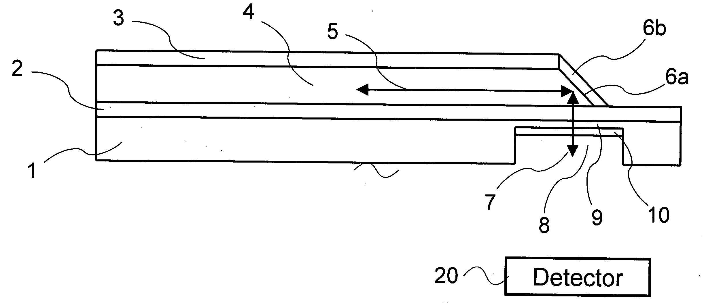
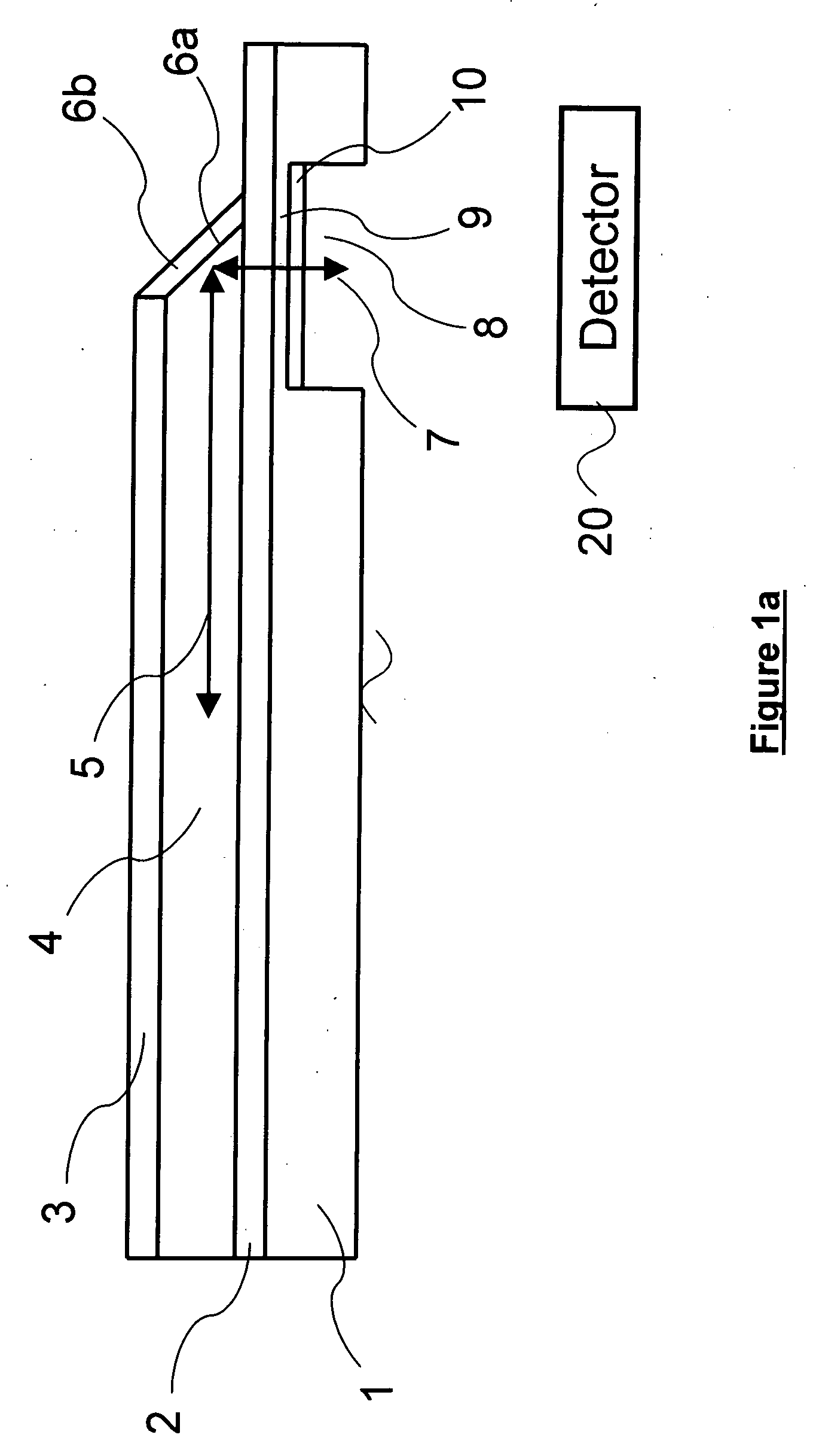
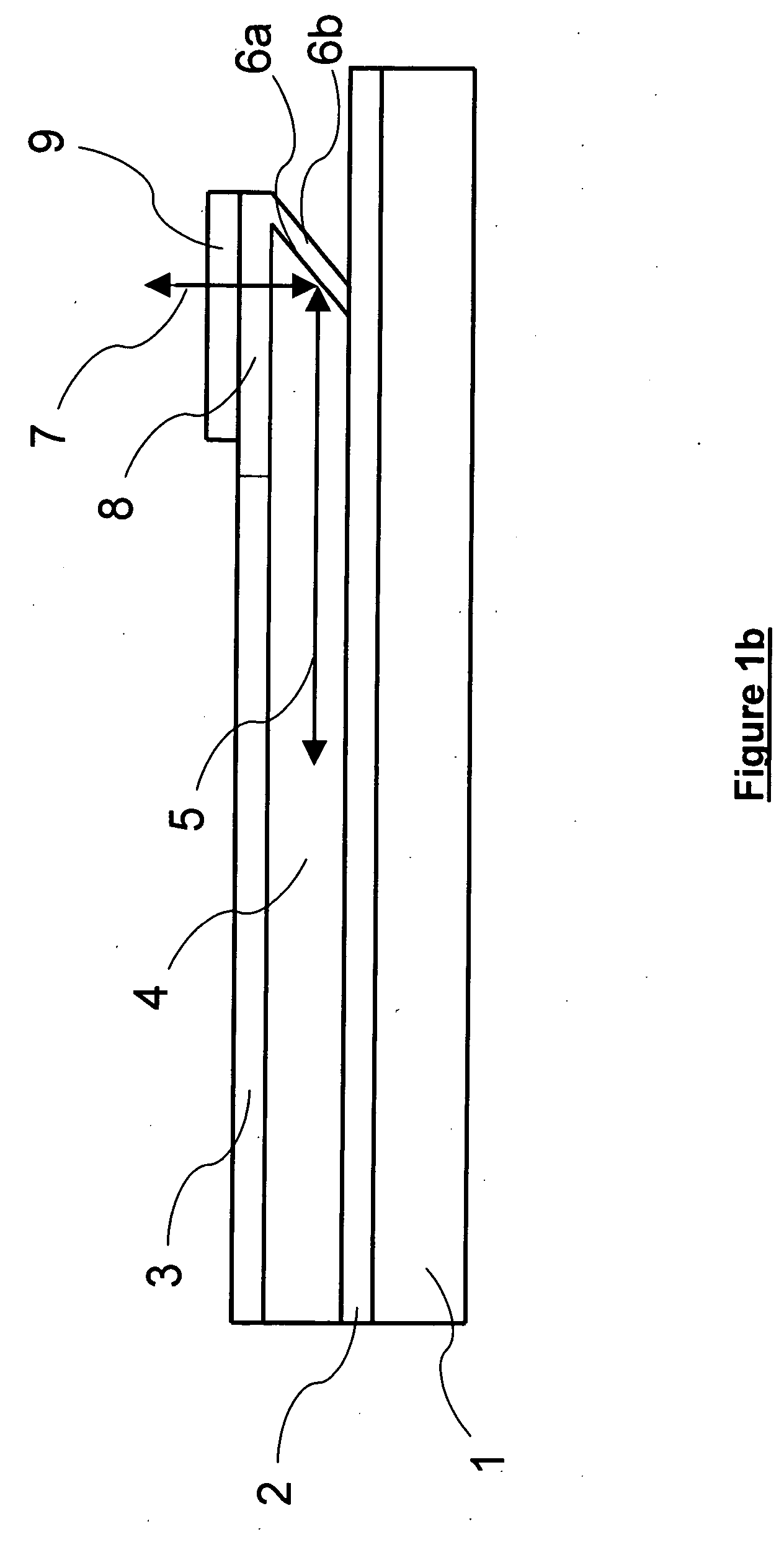
[0024] In FIG. 1a, a portion of a waveguide forming part of a multichannel device is shown in cross-section. The coupling device, which is integrated on chip, forms an extension of the multichannel device and comprises a substrate 1, a bottom cladding 2, an upper cladding 3 (optional), and a waveguide core 4. A guided wave 5 travels within the waveguide core 4 in a manner known per se. This waveguide core 4 terminates in a bevelled end 6a at a point short of the end of the bottom cladding 2

[0025] A reflection element in the form of a mirror facet 6a with optional cladding and reflective coating 6b is located at the bevelled end of the waveguide core 4.

[0026] A guided wave 5 travelling in the waveguide core 4 is redirected by the reflection element and emerges through aperture 8 as out-of-plane wave propagating in a direction approximately orthogonal to the plane of the waveguide core 4. To reduce loss due to Fresnel reflection, an antireflective layer 10 can be advantageously used....


PUM


Abstract

The multichannel waveguide device includes an array of waveguides located in a plane. Each waveguide channel has a redirecting element for redirecting a guided wave out of said plane, or vice versa. The redirecting elements are staggered in the direction of the waveguides so as to transform a one-dimensional array of in-plane waves into a two-dimensional array of out-of-plane waves, or vice versa.

Description

CROSS REFERENCE TO RELATED APPLICATION [0001] This invention claims the benefit under 35 USC 119(e) of prior U.S. provisional application 60 / 481,828 filed on Dec. 24, 2003.FIELD OF THE INVENTION [0002] This invention relates to the field of photonics, and in particular to optical off-chip interconnects in multichannel planar waveguide devices, and waveguide devices incorporating such interconnects. BACKGROUND OF THE INVENTION [0003] In a multichannel waveguide device, such as an integrated wavelength dispersive device (for example a planar waveguide microspectrometer) or an optical planar waveguide circuit containing multiple waveguides, there is an increasing demand to connect a large number of waveguides located on a single chip with output readout circuitry. A similar interconnection problem exists when optically coupling a large number of optical input ports, such as VCSELs (vertical cavity surface emitting lasers) or optical fibre arrays to a multichannel optical waveguide devi...

Claims


Application Information

Patent Timeline
Patent Type & Authority Applications(United States)
IPC IPC(8): G02B6/12G02B6/122G02B6/124G02B6/26G02B6/34G02B6/42
CPCG02B6/12019G02B6/122G02B6/425G02B6/4201G02B6/4214G02B6/124G02B6/4287
Inventor CHEBEN, PAVELJANZ, SIEGFRIEDLAMONTAGNE, BORISXU, DAN-XIA
Owner NAT RES COUNCIL OF CANADA
Why Eureka
Try Eureka