Display apparatus
a technology of display apparatus and display device, which is applied in the field of display device, can solve the problems of rewriting or changing the specific information of the display device, inhibiting the rewriting circuit, etc., and achieves the effect of improving usability and reliability of the display devi
- Summary
- Abstract
- Description
- Claims
- Application Information
AI Technical Summary
Benefits of technology
Problems solved by technology
Method used
Image
Examples
first embodiment
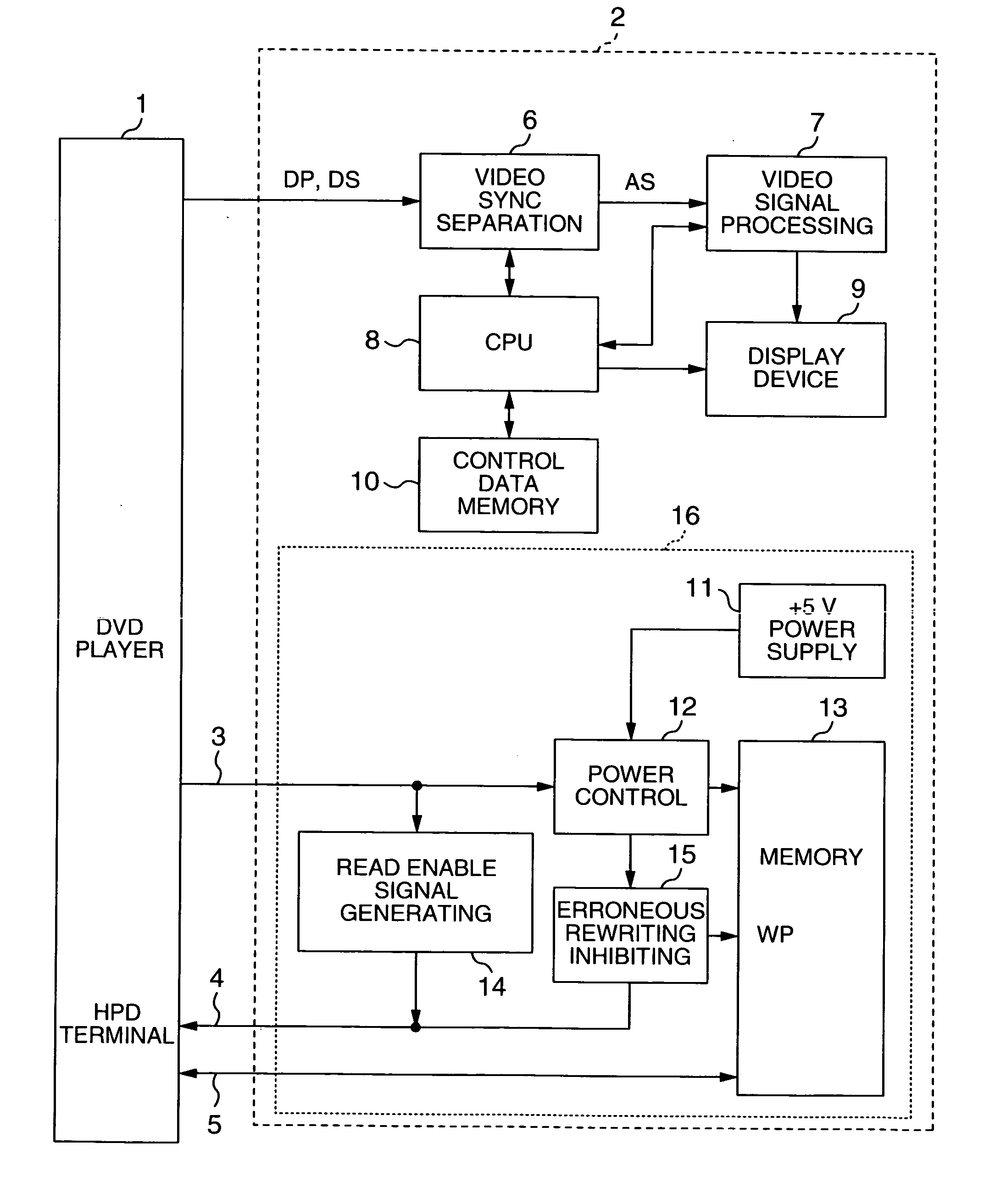
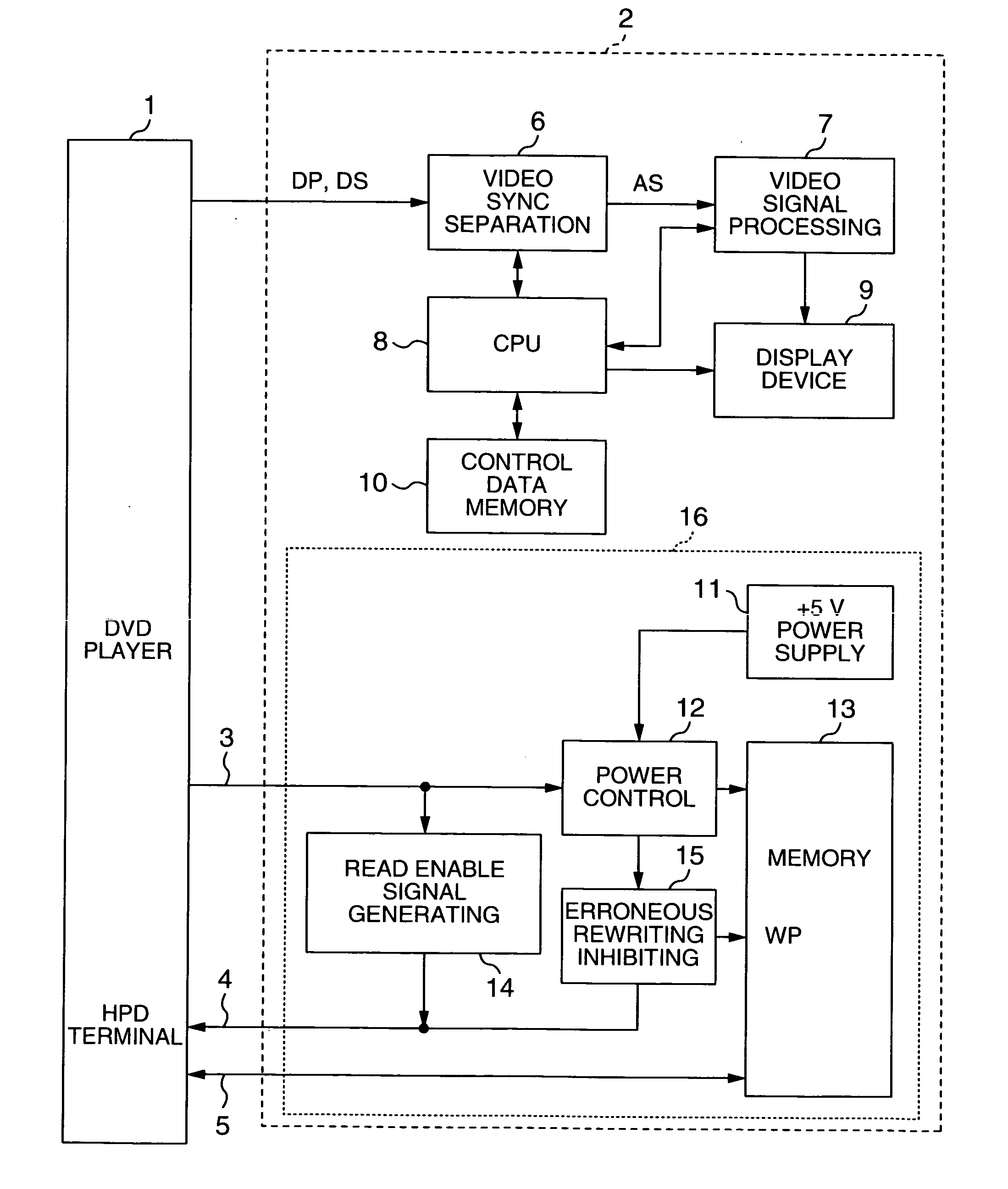
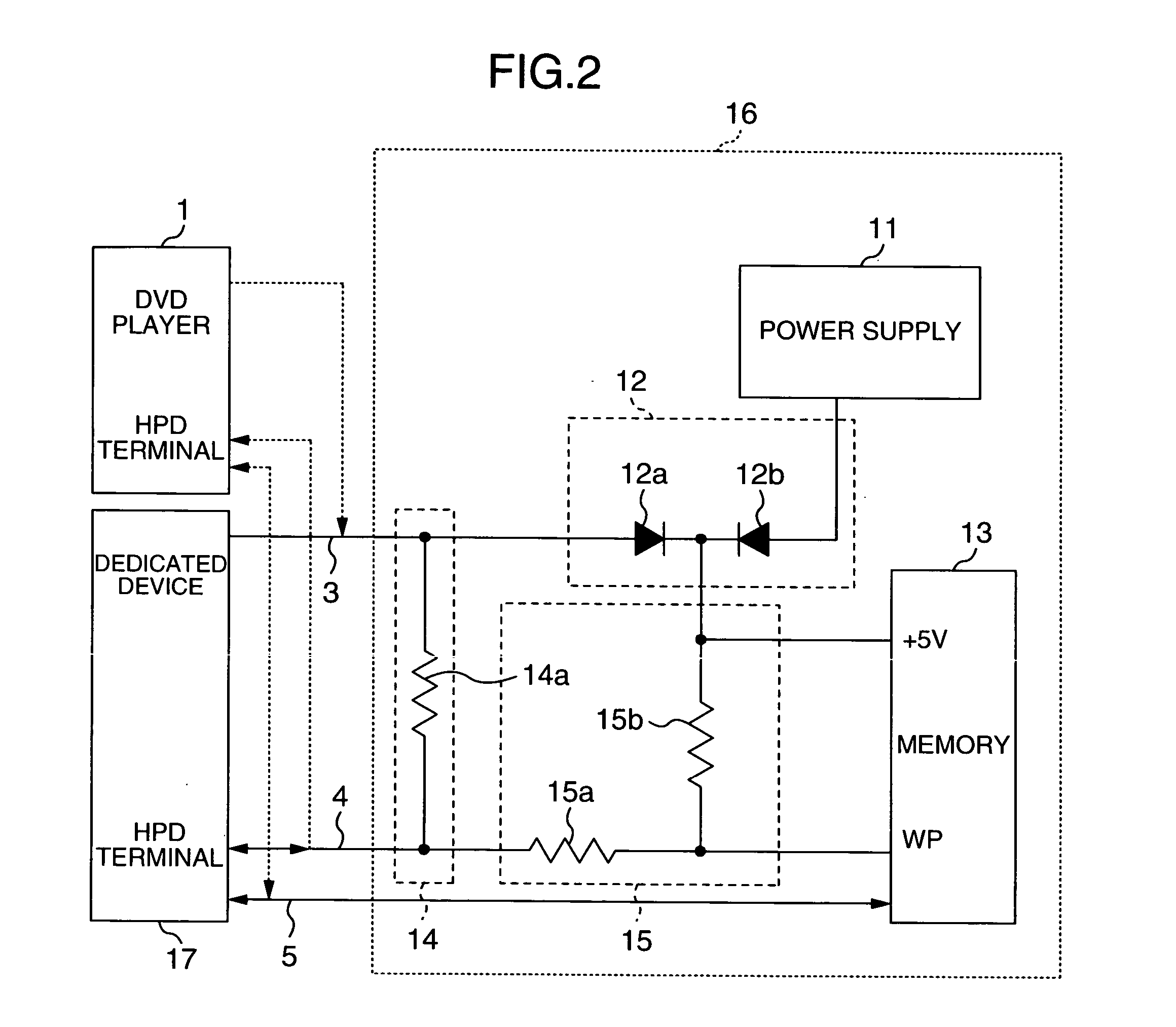
[0036]FIG. 2 is a block diagram showing a first embodiment of an erroneous rewriting inhibiting circuit 15 and its peripheral circuit, i.e., a write disable / enable control circuit 16 according to the present invention. The configuration includes directive elements, i.e., diodes 12a and 12b to establish an OR connection between the +5 V power source from the +5 V power line 3 and the +5 V power source in the display apparatus 2; resistors 14a, 15a, and 15b; and a particular dedicated unit 17 connected in place of the DVD player 1 when the specification information of the display apparatus 2 is written in the memory 13. The resistance values of resistors 15a and 15b are sufficiently larger than that of the resistor 14a. In FIG. 2, the same constituent components as those of FIG. 1 are assigned with the same reference numerals.
[0037] The memory 13 is a type of storage device including a control terminal WP to disable / enable a writing operation in an memory array thereof. The control s...
second embodiment
[0057] Next, description will be given of a second embodiment of the present invention. In the first embodiment, a voltage satisfying the write enabling condition for the write disable / enable control terminal of the memory is applied from the dedicated unit 17 to the read enable signal line (HPD line) 4. However, the present invention is not restricted only by the first embodiment. For example, in the configuration of FIG. 2, when the signal line (HPD line) 4 is set to an open state on the side of the dedicated unit 7 and a predetermined voltage similar to that described above is applied to the side of the +5 V power line 3, the memory can be set to the write enabled state for the following reason. That is, when the resistor 14a of the read enable signal generator 14 is sufficiently smaller in resistance than the resistors 15a and 15b included in the erroneous rewriting inhibiting circuit 15, the write enabling condition of expression (3) can be readily satisfied. This can be easily...
PUM
 Abstract
Description
Claims
Application Information


