Dual damascene process for forming a multi-layer low-K dielectric interconnect

a dielectric interconnect and damascene technology, applied in the direction of electrical equipment, semiconductor devices, semiconductor/solid-state device details, etc., can solve the problems of reducing overall fabrication steps, and high rc delay, so as to reduce the effective dielectric constant of damascene and reduce the speed delay of the ic

Inactive Publication Date: 2005-06-30
MACRONIX INT CO LTD
View PDF13 Cites 16 Cited by
  • Summary
  • Abstract
  • Description
  • Claims
  • Application Information

AI Technical Summary

Benefits of technology

[0006] One object of the present invention is to propose a process of forming a multi-layer Cu dual damascene interconnect to lower the effective dielectric constant thereof and thereby reduce the speed delay of the IC employing the multi-layer Cu dual damascene interconnect.

Problems solved by technology

In general, dual damascene process may reduce overall fabrication steps and copper-based conductor may effectively lower the resistance of wiring.
However, in an extremely high density IC, formation of dual damascene interconnect with Cu process still faces high RC delay due to high dielectric constant of the inter-layer dielectric (ILD), and delay of the IC in operation arises.
Utilization of low-k material for ILD may lower the effective dielectric constant of dual damascene interconnect.
However, this method of lowering the dielectric constant has its limitation.
Even though further lowering the effective dielectric constant, this process complicates the process as well and likewise, much lower dielectric constant material may not be applied in this process.
Unfortunately, spin-on low-k dielectric having dielectric constant lower than 2.5 is difficult to apply to large area, uniform or thicker deposition and hence, is not suitable for current dual damascene process.
In the process, spin-on low-k dielectrics are difficult to control and are only suitable for trench filling.
In other words, conventional dual damascene processes cannot make good use of spin-on low-k dielectrics to lower the effective dielectric constant of dual damascene interconnects.

Method used


Image

  • Dual damascene process for forming a multi-layer low-K dielectric interconnect
  • Dual damascene process for forming a multi-layer low-K dielectric interconnect
  • Dual damascene process for forming a multi-layer low-K dielectric interconnect

Examples


Embodiment Construction

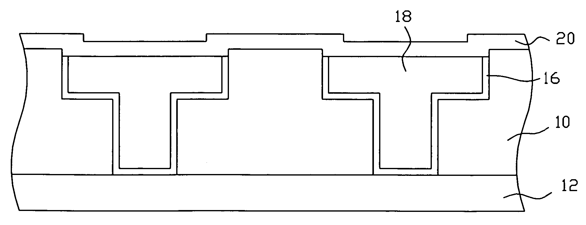
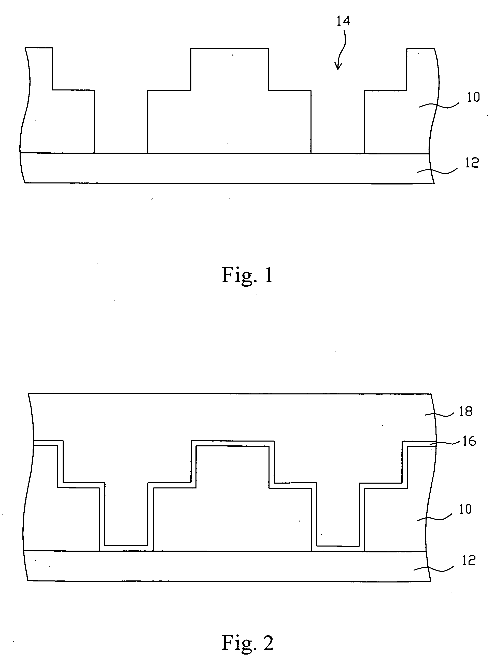
[0018]FIGS. 1-8 are provided to illustrate an embodiment dual damascene process of the present invention. As shown in FIG. 1, a dielectric layer 10 is deposited on a substrate 12 and then the dielectric layer 10 is etched to form dual damascene vias 14. The substrate 12 is referred as the layer underlying the dual damascene interconnect, for example some semiconductor materials and / or metallization layer that have manufactured with several electronic devices thereof. The dielectric layer 10 may be an oxide with dielectric constant around 3.5 or a SiOC formed by CVD that has a dielectric constant between 2.5 and 3.

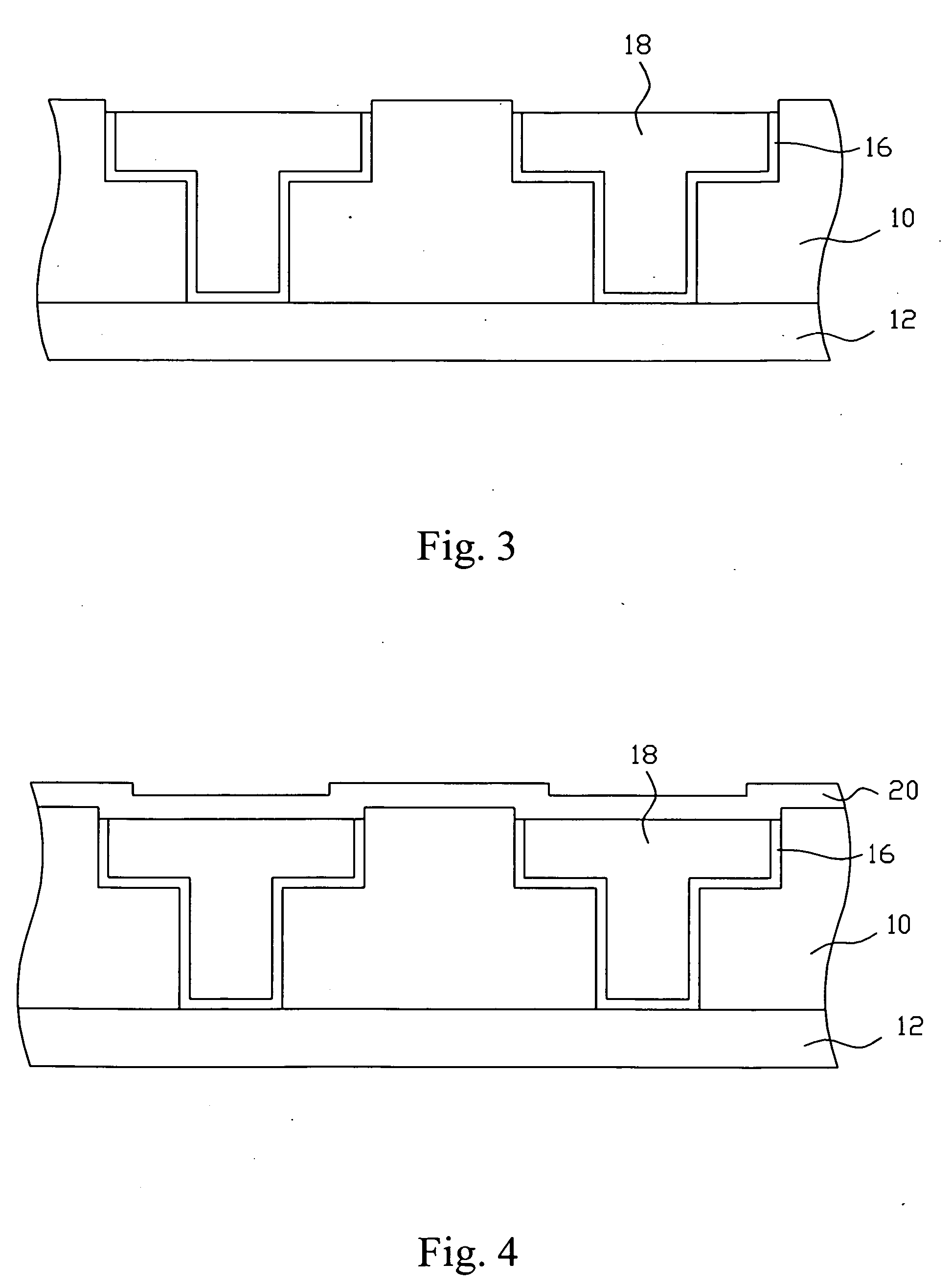
[0019] As shown in FIG. 2, a barrier layer 16 is formed and covered on the dielectric layer 10 and substrate 12, including the sidewall of the vias 14. The barrier layer 16 is made of materials capable of stopping Cu diffusion. Cu conductor 18 is then deposited to fill in the via 14. As shown in FIG. 3, the Cu conductor 18 and barrier layer 16 are etched back and thereby l...


PUM


Abstract

In a dual damascene process for forming a multi-layer low-k dielectric interconnect, the formation of each layer of interconnect comprises deposition of a first low-k dielectric layer, etching of the first low-k dielectric layer to form two dual damascene vias, formation of two Cu conductor plugs enclosed with barrier layers in the two dual damascene vias, etching of the first low-k dielectric layer between the two dual damascene vias to form a trench, and spin-on of a second low-k dielectric layer filled in the trench. The spin-on low-k dielectric layer is selected to have a dielectric constant smaller than that of the first low-k dielectric layer to reduce the equivalent dielectric constant in the layer of interconnect.

Description

FIELD OF THE INVENTION [0001] The present invention relates generally to a dual damascene process and structure, and more particularly to a dual damascene process for forming a multi-layer low-k dielectric interconnect. BACKGROUND OF THE INVENTION [0002] Due to the rapid development of integrated circuit (IC) process, the components in an IC are shrunk to attain high density. For the high density and shrinkage, it is required more advanced wiring structure and new materials for better transmission performance. Thus, copper-based conductor is employed to replace the traditional aluminum wiring. High density of IC increases difficulties to the process and therefore, dual damascene process and structure is developed to simplify the fabrication work. [0003] In general, dual damascene process may reduce overall fabrication steps and copper-based conductor may effectively lower the resistance of wiring. However, in an extremely high density IC, formation of dual damascene interconnect wit...

Claims


Application Information

Patent Timeline
Patent Type & Authority Applications(United States)
IPC IPC(8): H01L21/00H01L21/44H01L21/4763H01L21/768H01L23/532
CPCH01L21/76807H01L21/76835H01L23/5329H01L23/53238H01L21/76885H01L2924/0002H01L2924/00
Inventor TU, JUI-NENG
Owner MACRONIX INT CO LTD
Why Eureka
Try Eureka