Method for Reducing Thickness of Interfacial Layer, Method for Forming High Dielectric Constant Gate Insulating Film, High Dielectric Constant Gate Insulating Film, High Dielectric Constant Gate Oxide Film, and Transistor Having High Dielectric Constant Gate Oxide Film

a technology of interfacial layer and thickness, which is applied in the direction of electrical equipment, semiconductor devices, semiconductor/solid-state device details, etc., can solve the problems of increasing the oxygen void in the high dielectric film, the interfacial layer is not substantially solved, and the dielectric constant is not substantial

Inactive Publication Date: 2012-11-08
NAT INST FOR MATERIALS SCI
View PDF1 Cites 9 Cited by
  • Summary
  • Abstract
  • Description
  • Claims
  • Application Information

AI Technical Summary

Benefits of technology

[0012]An object of the present invention is to solve the aforementioned problem associated with an interfacial layer by thinning an interfacial layer, which has been formed beneath a high dielectric film without deteriorating the properties of the high dielectric film.
[0014]According to one aspect of the present invention, the following method for reducing a thickness of an interfacial layer is provided.
[0031]According to yet another aspect of the present invention, there is provided a high dielectric constant gate insulating film formed by any of the aforementioned aspects of the method for reducing a thickness of an interfacial layer.
[0041]The present invention can achieve the aforementioned object and reduce a thickness of an interfacial layer, and therefore effective dielectric constant of a gate insulating film can be maintained high in a device using a high dielectric oxide film as the gate insulating film.

Problems solved by technology

When such high dielectric oxide film is formed on a substrate of Si or Ge, an interfacial layer, such as SiOx and GeOx, is formed at the interface between the oxide film and the substrate to lower the effective dielectric constant, which is recognized as a problem.
There has been an attempt to further increase its dielectric constant by adding Ti to HfO2 (for example, Min Li, Zhihong Zhang, Stephen A. Campbella, Hong-Jyh Li and Jeff J. Peterson, “Hafnium titanate as a high permittivity gate insulator: Electrical and physical characteristics and thermodynamic stability,” JOURNAL OF APPLIED PHYSICS 101, 044509 (2007)), but it does not substantially solve the aforementioned problem associated with the interfacial layer.
This related art is however to control the threshold voltage by varying the effective work function of the electrode, not to solve the aforementioned problem associated with the interfacial layer.
Since this related art is to prevent oxygen from being diffused from outside of the oxide to the inside thereof, it cannot solve the aforementioned problem by the capping, once the interfacial layer is formed (as described above, an interfacial layer is easily formed).
By withdrawing oxygen from the interfacial layer in this manner, however, oxygen is also withdrawn from the high dielectric film, which increases oxygen voids in the high dielectric film.
The presence of the oxygen voids in the high dielectric film becomes a factor for deteriorating reliability of a device, and therefore it is not preferable to solve the aforementioned problem of the interfacial layer using this method.
When these inserted layers are oxidized (when an oxide layer is originally inserted, the oxide layer itself), the same problem as mentioned above is caused so that improvement in properties of a device produced from these semiconductors is inhibited.

Method used


Image

  • Method for Reducing Thickness of Interfacial Layer, Method for Forming High Dielectric Constant Gate Insulating Film, High Dielectric Constant Gate Insulating Film, High Dielectric Constant Gate Oxide Film, and Transistor Having High Dielectric Constant Gate Oxide Film
  • Method for Reducing Thickness of Interfacial Layer, Method for Forming High Dielectric Constant Gate Insulating Film, High Dielectric Constant Gate Insulating Film, High Dielectric Constant Gate Oxide Film, and Transistor Having High Dielectric Constant Gate Oxide Film
  • Method for Reducing Thickness of Interfacial Layer, Method for Forming High Dielectric Constant Gate Insulating Film, High Dielectric Constant Gate Insulating Film, High Dielectric Constant Gate Oxide Film, and Transistor Having High Dielectric Constant Gate Oxide Film

Examples


example 1

[0061]Here, an example for exhibiting an effect of reducing a thickness of an interfacial layer according to the present invention will be explained in comparison with a comparative example according to the conventional art.

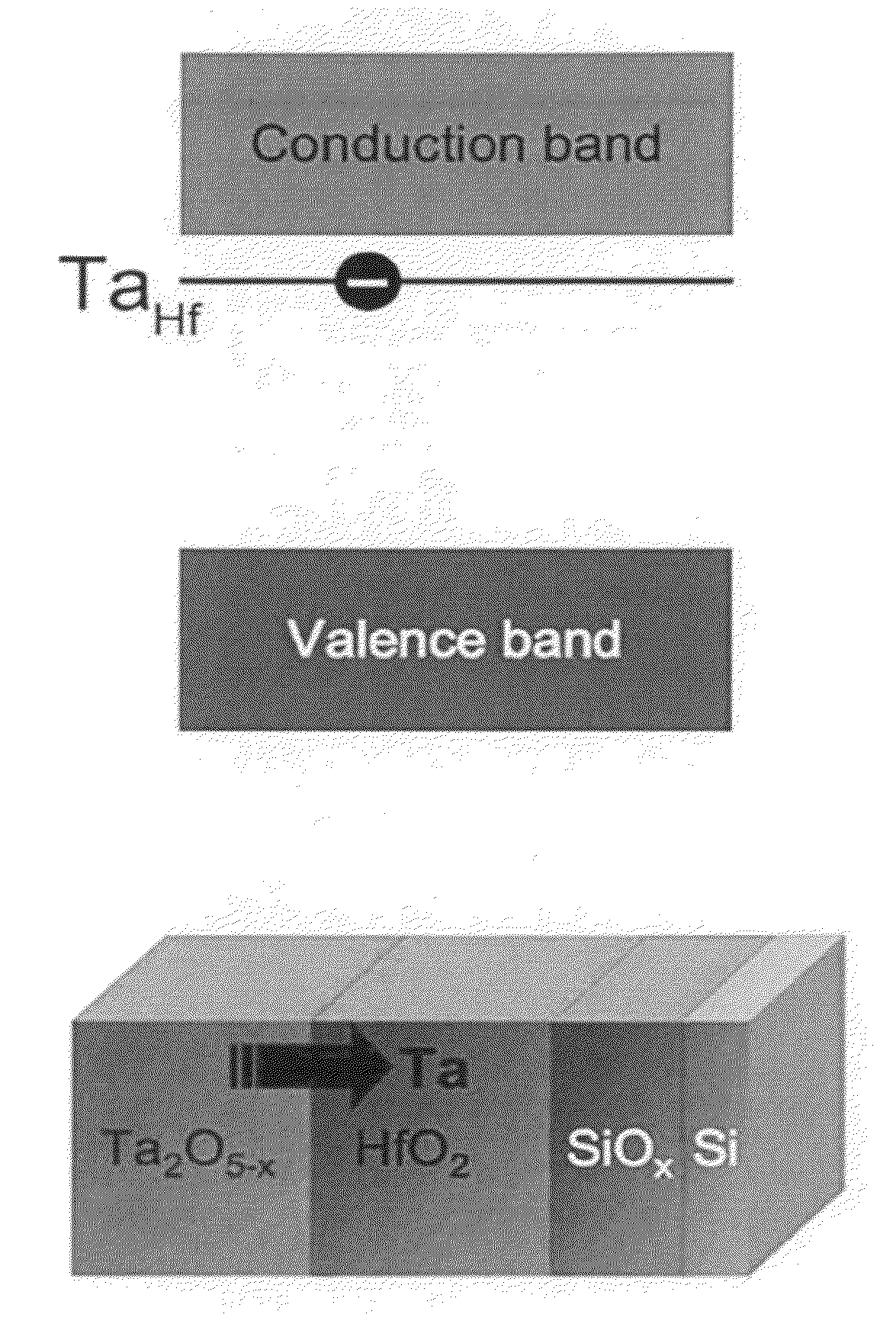
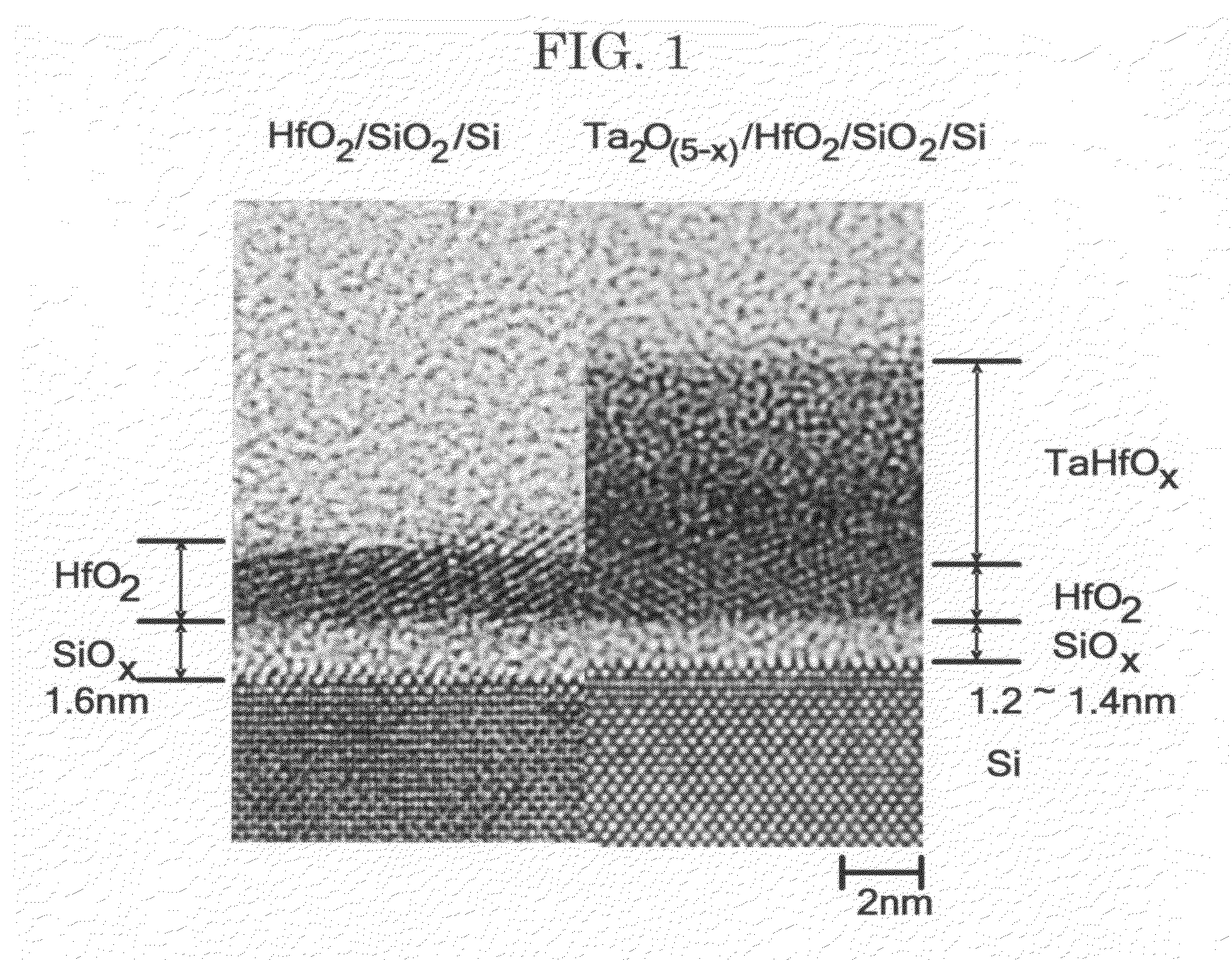
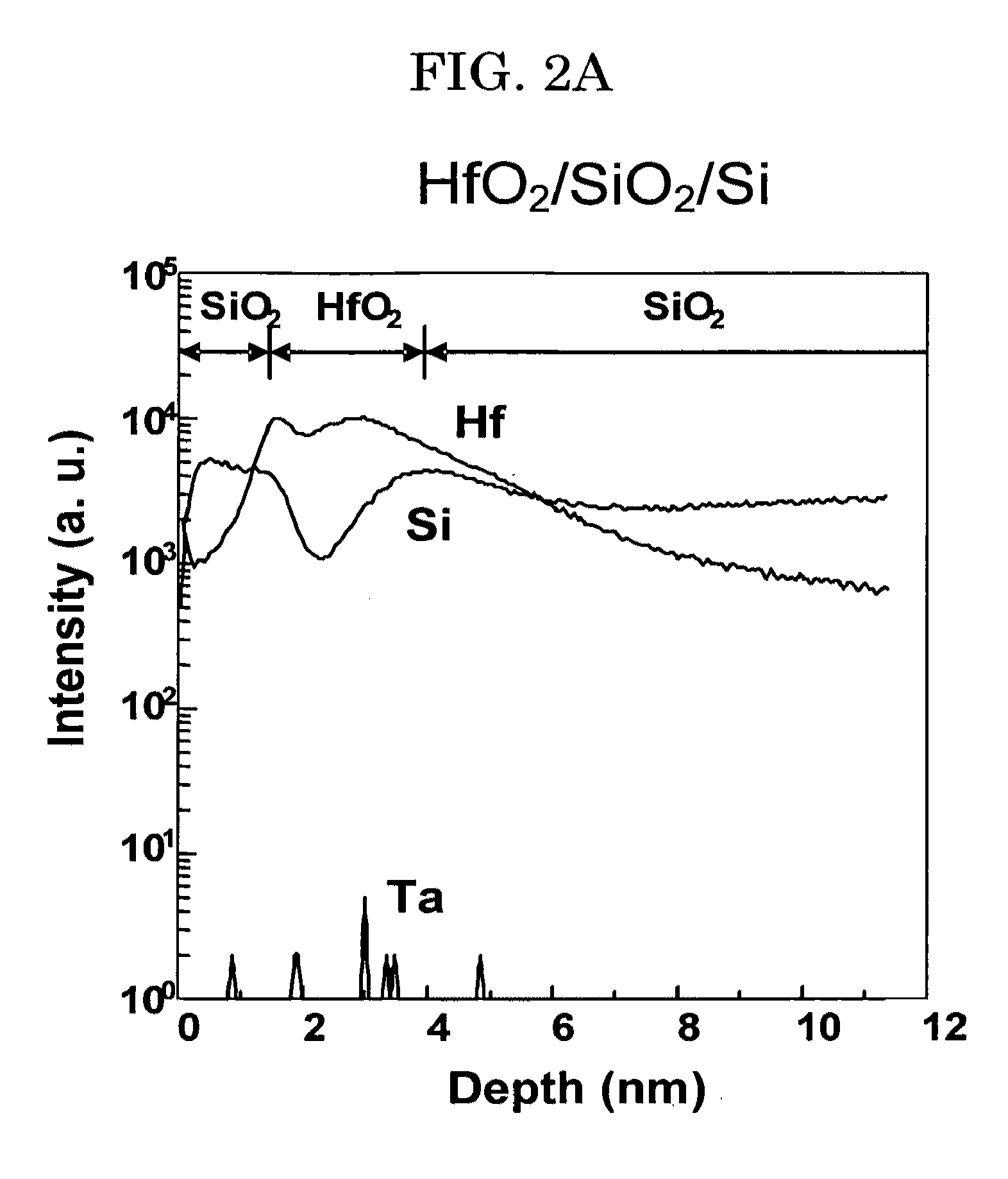
[0062]A right half of the photograph of FIG. 1 is a transmission electron microscopic (TEM) photograph of a cross-section of a layer structure produced in one example of the present invention. For the production of this layer structure, a thin silicon oxide (SiO2) film is formed on a Si substrate, followed by forming hafnium oxide (HfO2) film on the SiO2 film. Thereafter, a tantalum oxide (Ta2O5-x) film is formed on the HfO2 film (the reason for using Ta2O5-x, not Ta2O5, will be explained later).

[0063]A more specific production method of the aforementioned layer structure is as follows.

(1) Thin Silicon Oxide Film

[0064]After removing a natural oxide film on a surface of the Si substrate with a diluted hydrofluoric acid solution, the Si substrate was treated by sub...

example 2

[0092]An example where the present invention is applied to a production method of a complementary metal oxide semiconductor (CMOS) integrated circuit constituted of an n-channel and p-channel MOS transistors will be explained with reference to FIGS. 6 to 15. On the actual practice, numbers of transistors are formed on a semiconductor substrate, but in the following example, it is explained, for easiness in understanding, as if one n-channel MOS transistor and one p-channel MOS transistor are produced.

[0093]First, as illustrated in FIG. 6, for example, an element isolation trench 602 was formed in a main surface of a semiconductor substrate formed of a p-type monocrystal silicon (referred to as the substrate, hereinafter) 601 by the conventional shallow trench isolation technique.

[0094]Subsequently, an n-channel MOS transistor forming region (left half in the figure, which is the same in the following figures) of the substrate 601 was doped with boron by ion implantation, and a p-cha...


PUM

PropertyMeasurementUnit
temperatureaaaaaaaaaa
thicknessaaaaaaaaaa
thicknessaaaaaaaaaa

Abstract

To provide a method for reducing a thickness of an interfacial layer, which contains: (a) forming a film of an oxide of a first metal on a semiconductor layer via an oxide film of a semiconducdor serving as an interfacial layer; and (b) forming a film of an oxide of a second metal on the film of the oxide of the first metal, where the second metal has higher valency than that of the first metal.

Description

CROSS REFERENCE TO RELATED APPLICATIONS[0001]This application is continuation of PCT / JP2010 / 071353, filed on Nov. 30, 2010, the entire contents of which are incorporated herein by reference.BACKGROUND OF THE INVENTION[0002]1. Field of the Invention[0003]The present invention relates to a method for reducing a thickness of an interfacial layer, a method for forming a high dielectric constant gate insulating film, a high dielectric constant gate insulating film, a high dielectric constant gate oxide film, and transistor having a high dielectric constant gate oxide film, particularly relating to a method for controlling a structure of solid interface, and to a structure of a gate stack.[0004]2. Description of the Related Art[0005]Along the trends for miniaturizing elements on an integrated circuit, as a gate insulating film, an oxide film of high dielectric constant, such as HfO2 and La2O3, has been used, replacing the conventionally used silicon oxide.[0006]When such high dielectric o...

Claims


Application Information

Patent Timeline
Patent Type & Authority Applications(United States)
IPC IPC(8): H01L21/316H01L29/51
CPCH01L21/02181H01L21/02183H01L21/02194H01L21/022H01L21/02266H01L21/0228H01L29/51H01L21/823842H01L21/823857H01L29/513H01L29/517H01L29/7833H01L21/28194
Inventor UMEZAWA, NAOTOCHIKYO, TOYOHIRONABATAME, TOSHIHIDE
Owner NAT INST FOR MATERIALS SCI
Why Eureka
Try Eureka